Phase Splitter
1. Definition and Purpose of a Phase Splitter
Definition and Purpose of a Phase Splitter
A phase splitter is an electronic circuit that takes a single input signal and produces two output signals of equal amplitude but opposite phase (i.e., 180° apart). This functionality is critical in applications requiring balanced differential signals, such as push-pull amplifiers, bridge circuits, and certain types of analog signal processing systems.
Fundamental Operation
The phase splitter operates by generating two complementary signals from a single input. Mathematically, if the input signal is Vin(t) = A sin(ωt), the outputs are:
These outputs maintain the same frequency and amplitude but differ in phase by 180°. The negative sign in Vout2 indicates the phase inversion.
Key Characteristics
- Balanced Outputs: The amplitudes of both outputs must be precisely matched to avoid distortion in downstream circuits.
- High Input Impedance: Minimizes loading effects on the preceding stage.
- Low Output Impedance: Ensures the phase splitter can drive subsequent stages effectively.
Common Implementations
Several circuit topologies achieve phase splitting, each with distinct advantages:
1. Differential Amplifier
A differential amplifier with a single-ended input naturally produces two anti-phase outputs. The gain and phase accuracy depend on the symmetry of the transistor or op-amp pair.
2. Transformer-Based Splitter
A center-tapped transformer inherently provides two out-of-phase signals. While highly linear, transformers introduce frequency-dependent phase shifts and are bulky for integrated designs.
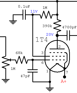
3. Cathode/Emittor Follower Pair
Used in vacuum tube and bipolar transistor designs, this method employs a common-cathode (or common-emitter) stage followed by a cathode/emitter follower to generate the inverted and non-inverted signals, respectively.
Practical Applications
Phase splitters are indispensable in:
- Push-Pull Amplifiers: Ensures the two amplifying devices receive properly phased signals for efficient power delivery.
- Modulation/Demodulation Circuits: Used in balanced mixers and synchronous detectors to suppress carrier signals.
- Test Equipment: Generates complementary signals for differential measurements.
Mathematical Analysis of a Resistive Phase Splitter
Consider a simple resistive phase splitter using an op-amp:
For balanced outputs, the gains must satisfy:
This condition is met when Rf = Ri, yielding equal-magnitude outputs of opposite phase.
1.2 Key Applications in Electronics
Push-Pull Amplifiers
Phase splitters are fundamental in push-pull amplifier configurations, where they generate two anti-phase signals to drive complementary transistor pairs. The balanced output ensures minimal distortion by canceling even-order harmonics. A common implementation uses a long-tailed pair or a paraphase inverter to achieve the required 180° phase shift. The output impedance matching between the two phases is critical to maintain symmetry and prevent crossover distortion.
Modulation and Demodulation Circuits
In single-sideband (SSB) modulation, phase splitters enable the generation of quadrature signals necessary for phasing-type SSB modulators. The Hilbert transform, approximated using all-pass filter networks, relies on precise phase splitting to isolate the upper and lower sidebands. Similarly, in synchronous demodulation, phase splitters recover the in-phase (I) and quadrature (Q) components of a signal, essential for coherent detection in software-defined radios.
Instrumentation and Measurement
Phase splitters are integral to lock-in amplifiers, where they provide reference signals for phase-sensitive detection. By splitting a reference oscillator signal into two paths with a controlled phase relationship, lock-in amplifiers can measure extremely small signals buried in noise. The phase accuracy, typically within ±0.1°, directly impacts the measurement sensitivity.
Audio Engineering
In stereo audio systems, phase splitters create balanced line-level signals to reduce noise pickup in long cable runs. The Schmitt trigger-based phase splitter is particularly effective for converting unbalanced signals to differential outputs while maintaining high common-mode rejection ratios (CMRR > 60 dB). This technique is widely used in professional audio interfaces and microphone preamplifiers.
Power Electronics
Three-phase inverters utilize phase splitters to generate 120°-shifted gate drive signals for MOSFET/IGBT bridges. The splitter’s bandwidth must exceed the switching frequency to prevent timing skew, which can lead to shoot-through currents. Digital implementations using phase-locked loops (PLLs) with fractional-N dividers offer sub-nanosecond phase resolution for high-frequency applications.
Case Study: Phase Splitter in RF Mixers
A double-balanced mixer requires precise anti-phase local oscillator (LO) signals to suppress carrier leakage. A transformer-based phase splitter with center-tapped secondary windings is often employed, providing inherent amplitude balance. For frequencies above 1 GHz, Lange couplers or rat-race hybrids replace traditional splitters, offering broadband performance with phase errors below 5° across octave bandwidths.
1.3 Basic Operating Principles
A phase splitter is a circuit that generates two output signals of equal amplitude but opposite phase (180° apart) from a single input signal. This functionality is essential in push-pull amplifiers, balanced modulators, and differential signaling systems. The core principle relies on symmetrical signal inversion and amplification.
Mathematical Derivation of Phase Splitting
Consider an input signal Vin applied to a phase splitter. The outputs Vout1 (non-inverting) and Vout2 (inverting) must satisfy:
where Av is the voltage gain. For ideal operation, the magnitudes must match:
Common Topologies
1. Differential Pair Phase Splitter
A long-tailed pair with matched transistors generates complementary outputs. The collector currents IC1 and IC2 are related by:
where VT is the thermal voltage (≈26 mV at 300 K). The output voltages at the collectors are 180° out of phase.
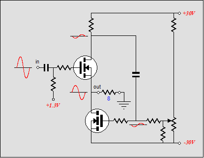
2. Cathodyne (Split-Load) Phase Splitter
This vacuum tube or FET-based circuit splits phase via a shared load resistor. The voltage division ensures:
where μ is amplification factor, rp is plate resistance, and Rk is the cathode resistor.
Practical Considerations
- Impedance matching: Output impedances must be balanced to prevent phase or amplitude errors.
- Frequency response: Stray capacitances can cause phase deviations at high frequencies.
- DC biasing: Proper quiescent point setting avoids distortion in the output waveforms.
Real-World Applications
Phase splitters are critical in:
- Class B push-pull audio amplifiers
- RF balanced mixers
- Differential ADCs and DACs
- Telecommunication line drivers
2. Transformer-Based Phase Splitters
Transformer-Based Phase Splitters
Transformer-based phase splitters leverage the inherent electromagnetic coupling of transformers to generate two or more output signals with precise phase relationships. These circuits are widely used in power electronics, audio amplification, and RF systems where phase accuracy and isolation are critical.
Operating Principle
A transformer with a center-tapped secondary winding naturally produces two outputs that are 180° out of phase. When an AC signal is applied to the primary winding, the induced voltages at the secondary winding's ends (relative to the center tap) exhibit equal magnitude but opposite polarity. The phase relationship arises from the winding direction and transformer action.
Here, N1 and N2 represent the primary and secondary turns, respectively. The negative sign indicates the phase inversion.
Key Design Considerations
Transformer-based phase splitters must account for several critical parameters:
- Turn ratio: Determines voltage scaling between primary and secondary windings.
- Leakage inductance: Affects high-frequency response and phase accuracy.
- Core material: Influences saturation characteristics and frequency range.
- Winding capacitance: Impacts bandwidth and signal integrity.
Practical Implementation
In push-pull audio amplifiers, transformer phase splitters ensure balanced drive signals for the output stage. The center-tapped secondary provides a reference point, while the outer terminals deliver anti-phase signals to the power transistors. Proper impedance matching is essential to minimize reflections and maintain signal fidelity.
This equation ensures optimal power transfer by matching the reflected impedance to the source.
Advantages and Limitations
Advantages:
- Galvanic isolation between input and output stages.
- Inherent common-mode noise rejection.
- No active components required, enhancing reliability.
Limitations:
- Limited bandwidth due to parasitic elements.
- Nonlinearity at high flux densities.
- Size and weight constraints in compact designs.
Historical Context
Early vacuum tube amplifiers relied heavily on transformer phase splitters due to their simplicity and effectiveness. Modern applications often replace them with active circuits in low-power scenarios, but they remain indispensable in high-voltage and high-current systems.
Modern Applications
Transformer phase splitters are still prevalent in:
- RF balanced mixers and modulators.
- Three-phase power converters.
- Precision instrumentation requiring isolated signals.
2.2 Transistor-Based Phase Splitters
Basic Operating Principle
A transistor-based phase splitter generates two output signals of equal amplitude but opposite phase (180° apart) from a single input signal. The most common configurations use bipolar junction transistors (BJTs) or field-effect transistors (FETs) in a common-emitter (CE) or common-source (CS) arrangement with a split-load resistor network. The phase inversion arises from the inherent property of CE/CS amplifiers, where the output at the collector/drain is inverted relative to the input, while the emitter/source follows the input signal in phase.
Common-Emitter Phase Splitter
The simplest BJT phase splitter consists of a single transistor in a CE configuration with two load resistors: one at the collector (RC) and one at the emitter (RE). For symmetric outputs, RC = RE. The voltage gain from base to collector is:
where re is the transistor's intrinsic emitter resistance (~25 mV/IE). The emitter follower gain is:
When RC = RE, the magnitudes of Av,C and Av,E become nearly equal, producing balanced anti-phase outputs. However, the emitter output has a lower output impedance (Zout,E ≈ RE || (re + Rsource/β)) compared to the collector output (Zout,C ≈ RC).
Differential Pair Phase Splitter
For improved balance and linearity, a differential pair can be used. Here, the input drives one transistor's base, while the other base is grounded (or biased at a fixed voltage). The outputs taken from the two collectors provide inherently anti-phase signals. The differential gain is:
where gm is the transconductance. This configuration minimizes even-order harmonics and offers better common-mode rejection compared to single-transistor splitters.
Practical Considerations
- Impedance Matching: The unequal output impedances in single-transistor splitters can cause amplitude mismatches when driving unequal loads. Buffering with emitter followers may be necessary.
- DC Biasing: The quiescent current must be set to avoid clipping. For a CE splitter, VCC ≥ 2ICRC + VCE,sat ensures headroom.
- Frequency Response: The high-pass cutoff is determined by the input coupling capacitor and base impedance: fc = 1/(2πRB||(β+1)(re+RE)Cin).
Real-World Applications
Transistor phase splitters are fundamental in push-pull amplifiers, balanced modulators, and bridge output stages. For instance, the Long-Tailed Pair (a differential pair with a constant current source) is widely used in operational amplifier input stages and RF mixers where phase accuracy is critical. Modern implementations often replace discrete transistors with integrated op-amps or dedicated driver ICs for improved performance.
2.3 Op-Amp-Based Phase Splitters
Operational amplifiers (op-amps) provide a precise and flexible means of generating phase-split signals, particularly in applications requiring high input impedance, low output impedance, and minimal phase error. Unlike passive phase splitters, op-amp-based designs mitigate loading effects and maintain signal integrity across a broad frequency range.
Basic Inverting and Non-Inverting Configuration
The simplest op-amp phase splitter employs an inverting amplifier alongside a unity-gain buffer. The inverting amplifier produces a 180° phase shift with gain determined by the feedback network, while the non-inverting path preserves the original phase. For a balanced output, the inverting stage is configured with a gain of −1.
where Rf and Rin are the feedback and input resistors, respectively. Matching Rf = Rin ensures equal magnitudes for both outputs.
Differential Amplifier as a Phase Splitter
A differential amplifier configuration inherently generates complementary outputs. By setting R1 = R2 and R3 = R4, the circuit yields:
For symmetric outputs (Vout+ = −Vout−), the resistor ratios must satisfy R2/R1 = R4/R3.
Active Wien Bridge Phase Splitter
For applications requiring quadrature outputs (90° phase difference), an active Wien bridge network combines an op-amp integrator and differentiator. The integrator introduces a −90° phase shift, while the differentiator provides +90°:
where s = jω. At the center frequency (ω = 1/RC), the magnitudes are equal, and the phase difference is exactly 90°.
Practical Considerations
- Bandwidth Limitations: Op-amp slew rate and gain-bandwidth product constrain high-frequency performance.
- Component Tolerances: Mismatched resistors degrade phase accuracy; use 0.1% tolerance or laser-trimmed parts.
- Power Supply Rejection: Dual supplies are preferred to avoid DC offset in single-supply designs.
Applications
Op-amp phase splitters are critical in:
- Analog Signal Processing: Quadrature modulation/demodulation in communication systems.
- Audio Engineering: Balanced line drivers and noise-canceling circuits.
- Instrumentation: Lock-in amplifiers requiring precise phase references.
3. Circuit Configurations and Schematics
3.1 Circuit Configurations and Schematics
Common-Cathode (Differential) Phase Splitter
The common-cathode phase splitter, also known as a differential amplifier, utilizes two active devices (vacuum tubes or transistors) with a shared cathode (or emitter) resistor. The input signal is applied to one device, while the other provides an inverted output. The phase inversion arises due to the balanced current flow through the shared resistor, ensuring equal but opposite voltage swings at the anodes (or collectors).
where gm is the transconductance and RL the load resistor. The circuit’s symmetry ensures minimal phase distortion, making it ideal for push-pull amplifier stages.
Paraphase (Split-Load) Phase Splitter
In a paraphase configuration, a single active device drives two outputs: one taken directly from the anode (or collector) and another from a voltage divider at the cathode (or emitter). The cathode follower action provides a non-inverted signal, while the anode output is inverted. The voltage divider ratio must precisely match the gain to ensure equal-amplitude outputs.
for vacuum tubes, where μ is the amplification factor. Transistor implementations replace μ with β (current gain).
Long-Tailed Pair Phase Splitter
This variant enhances common-mode rejection by using a high-impedance tail resistor (or current source) in the shared cathode/emitter path. The tail forces constant combined current, ensuring that input signals drive the devices differentially. The outputs remain 180° out of phase, with amplitude matching dependent on device symmetry.
where Ad is the differential gain and Rk the tail resistance. Modern implementations often replace Rk with a current mirror for improved stability.
Transformer-Based Phase Splitters
Center-tapped transformers inherently provide anti-phase signals due to their winding configuration. While less common in solid-state designs, they remain prevalent in tube amplifiers for impedance matching and galvanic isolation. The output phases are inherently balanced, though bandwidth limitations arise from parasitic inductance and capacitance.
Practical Considerations
- Component Matching: Mismatched resistors or transistors degrade phase and amplitude balance, introducing distortion.
- Frequency Response: Stray capacitance in paraphase dividers or transformer windings can cause phase shifts at high frequencies.
- Power Supply Rejection: Differential pairs with current-source tails minimize supply noise coupling.
3.2 Signal Fidelity and Phase Accuracy
Fundamental Constraints in Phase Splitting
The primary challenge in phase splitting lies in maintaining signal fidelity while ensuring precise phase accuracy between the outputs. Any deviation from ideal behavior introduces distortion, compromising the integrity of the signal in applications such as quadrature modulation or differential signaling. The two critical parameters governing performance are:
- Amplitude Matching – The outputs must exhibit equal magnitudes to prevent imbalance.
- Phase Deviation – The phase difference between outputs must remain exactly 180° (or 90° for quadrature splitters) across the operating bandwidth.
Mathematical Analysis of Phase Error
For a differential phase splitter, the outputs Vout+ and Vout− should ideally satisfy:
However, non-idealities introduce amplitude imbalance (ΔA) and phase error (Δϕ):
The resulting phase imbalance is quantified as the deviation from the ideal 180° separation. For small errors (Δϕ ≪ 1 rad), the normalized phase error is:
Sources of Degradation
1. Component Tolerances
Passive splitters (e.g., resistor-based or transformer-coupled) suffer from parasitic capacitance (Cp) and inductance (Lp), causing frequency-dependent phase shifts. For a resistive splitter with mismatched resistors R1 ≠ R2, the phase error scales as:
2. Active Circuit Limitations
In op-amp or transistor-based splitters, finite bandwidth and slew rate induce phase lag. For a differential amplifier with pole frequency fp, the phase error at frequency f is:
Mitigation Techniques
- Negative Feedback – Reduces phase error by correcting output deviations in real-time.
- Trimmable Components – Laser-trimmed resistors or variable capacitors compensate for mismatches.
- Balanced Topologies – Fully differential architectures (e.g., Gilbert cells) inherently reject common-mode phase drift.
Case Study: High-Fidelity Splitting in RF Systems
In a 2.4 GHz quadrature splitter, a 5° phase error degrades image rejection by 20 dB. Modern designs use lumped-element Wilkinson dividers with λ/4 transmission lines to achieve Δϕ < 1° up to 6 GHz. Calibration algorithms further correct residual errors using DSP-based feedback.
3.3 Load Considerations and Impedance Matching
Output Loading Effects
The performance of a phase splitter is critically dependent on the load impedance presented at its outputs. An unbalanced load disrupts the symmetry of the anti-phase signals, introducing amplitude and phase errors. For a differential output stage, the output impedance Zout of each leg must satisfy:
where ZL is the load impedance. For a cathode-follower-based phase splitter, the output impedance is approximated by:
where gm is the transconductance and rp is the plate resistance. Loading effects become pronounced when driving capacitive loads, as the high-frequency roll-off is asymmetrically affected.
Impedance Matching Techniques
To maintain signal integrity, the following matching strategies are employed:
- Active Buffering: Adding unity-gain buffers (e.g., emitter followers) isolates the phase splitter from low-impedance loads.
- Transformer Coupling: A center-tapped transformer provides inherent impedance transformation while preserving phase symmetry.
- Resistive Balancing: Dummy loads equalize the effective impedance seen by both outputs.
For transformer-coupled designs, the turns ratio N must be selected to match the load impedance ZL to the optimal plate load Zopt:
Case Study: Long-Tailed Pair Phase Splitter
In a long-tailed pair configuration, the tail current IT and load resistors RL determine the output balance. Mismatched loads cause differential gain asymmetry, quantified by:
Modern implementations often use current mirrors to enforce symmetry, achieving load-independent phase splitting up to the mirror's bandwidth limit.
4. Common Design Challenges
4.1 Common Design Challenges
Phase Imbalance Due to Component Tolerances
A fundamental challenge in phase splitter design is maintaining precise 180° phase separation between outputs. Passive component mismatches—particularly in resistors and capacitors—introduce phase errors. For a differential amplifier-based splitter, even a 1% tolerance mismatch in collector or drain resistors (RC or RD) can degrade phase accuracy by several degrees. The phase error (Δϕ) scales with the mismatch ratio:
Where ΔR is the resistance deviation. In high-frequency applications (>10 MHz), parasitic capacitances exacerbate this effect by introducing additional phase shifts.
Output Amplitude Mismatch
Achieving equal-amplitude antiphase signals requires symmetric gain paths. In transistor-based splitters (e.g., long-tailed pair), VBE mismatches or Early voltage effects cause amplitude asymmetry. For FET implementations, threshold voltage (Vth) variations produce similar imbalances. The normalized amplitude error (εA) is:
Practical mitigation: Degeneration resistors reduce sensitivity to device mismatches but at the cost of reduced gain.
Power Supply Rejection Ratio (PSRR) Limitations
Phase splitters in single-supply configurations suffer from poor PSRR, as supply noise couples asymmetrically into the differential outputs. A 100 mV ripple on a 5V supply may induce >5° phase skew in uncompensated designs. The PSRR degradation factor (KPSRR) for a BJT differential pair is:
Where gm is transconductance, ro the output impedance, and RE the emitter degeneration resistance.
Thermal Drift Effects
Temperature gradients across the splitter circuit cause differential thermal drift. In IC implementations, localized heating from adjacent components can create >0.1%/°C gain variation between phases. For precision applications, thermal symmetry must be maintained through layout techniques like common-centroid placement or dummy structures.
High-Frequency Phase Error
Above the circuit's dominant pole frequency, parasitic phase shifts accumulate. The cumulative phase error (ϕerr) at frequency f is:
Where fpn and fzm are pole and zero frequencies. Above 100 MHz, transmission line effects in PCB traces further degrade performance unless matched-length routing is employed.
Load Sensitivity
Uneven loading between outputs disrupts phase balance. A 10% difference in load impedance can introduce 2–8° phase error depending on topology. Active buffering or impedance scaling networks (e.g., L-pads) are often necessary for driving mismatched loads.
4.2 Performance Optimization Techniques
Balanced Output Impedance
For optimal performance in a phase splitter, the output impedances of the inverting and non-inverting outputs must be matched. Mismatched impedances introduce phase and amplitude errors, degrading signal fidelity. Consider a differential amplifier phase splitter with emitter resistors RE. The output impedance at each terminal is given by:
where RC is the collector resistor, ro is the transistor's output resistance, and gm is the transconductance. To balance the outputs, RC and RE must be carefully selected such that Zout+ ≈ Zout-.
Minimizing Phase Error
Phase error arises from unequal propagation delays between the two outputs. In a long-tailed pair configuration, this can be mitigated by:
- Using matched transistor pairs with identical β and VBE characteristics.
- Employing a current mirror load to ensure symmetrical current splitting.
- Reducing parasitic capacitances by minimizing trace lengths and using high-frequency PCB materials.
The phase error Δφ can be approximated as:
where ΔC is the capacitance mismatch and ω is the angular frequency.
Amplitude Matching
Amplitude imbalance is primarily caused by resistor tolerances and transistor mismatches. For a differential phase splitter, the gain mismatch ΔA between outputs is:
To minimize ΔA:
- Use 1% or better tolerance resistors for RC and RE.
- Implement active feedback with an operational amplifier to dynamically correct gain errors.
- Thermally couple transistors to reduce VBE drift disparities.
Frequency Response Optimization
The bandwidth of a phase splitter is limited by the dominant pole formed by the load resistance and parasitic capacitance. The -3 dB frequency f3dB is:
where Ctotal = Cout + Cstray + Cload. Techniques to extend bandwidth include:
- Using cascode configurations to reduce Miller capacitance.
- Implementing peaking inductors to compensate for capacitive roll-off.
- Selecting transistors with high fT for the target frequency range.
Noise Reduction Strategies
Phase splitters in low-noise applications require careful attention to thermal and flicker noise. The input-referred noise voltage spectral density is:
where Kf and a are flicker noise coefficients. Noise can be reduced by:
- Using low-noise transistors with high β to minimize base current IB.
- Employing degeneration resistors to linearize gm without excessive thermal noise penalty.
- Implementing correlated double sampling in switched-capacitor phase splitters.
Power Supply Rejection Ratio (PSRR) Enhancement
Poor PSRR allows supply noise to modulate the output phases. For a resistively-loaded differential pair, the PSRR is:
Improvements can be achieved by:
- Using regulated supply voltages with low output impedance.
- Implementing current-source loads instead of resistive loads.
- Adding bypass capacitors with low ESR at critical nodes.
4.3 Debugging and Signal Integrity Issues
Common Signal Integrity Challenges in Phase Splitters
Phase splitters, particularly those based on differential amplifiers or transformer-coupled designs, are susceptible to signal integrity degradation due to mismatched impedances, parasitic capacitances, and inductive coupling. The primary issues include:
- Phase imbalance: Deviations from the ideal 180° separation due to component tolerances or asymmetrical layout.
- Amplitude mismatch: Unequal output magnitudes caused by load impedance variations or active device nonlinearities.
- Harmonic distortion: Introduced by saturation in transformer cores or clipping in transistor-based designs.
- Ground bounce: High-frequency return current paths disrupting reference planes in PCB implementations.
Quantifying Phase and Amplitude Errors
The phase error (Δφ) and amplitude imbalance (ΔA) between outputs can be modeled as:
where Zdiff and Zcm are the differential and common-mode impedances respectively. For transformer-based splitters, the phase error is dominated by the winding capacitance (Cw) and leakage inductance (Llk):
Debugging Methodology
Time-domain analysis: Use differential probes to capture both outputs simultaneously, checking for:
- Rise/fall time symmetry (should match within 5% for high-speed applications)
- Propagation delay matching (critical for RF and clock distribution)
- Overshoot/ringing (indicative of impedance discontinuities)
Frequency-domain analysis: Network analyzer measurements reveal:
- Common-mode rejection ratio (CMRR) degradation above cutoff frequency
- Parasitic resonance peaks from stray LC elements
- Skin effect losses in transformer windings at high frequencies
Layout Considerations for High-Fidelity Splitting
For PCB implementations, maintain:
- Symmetrical trace lengths (±1% tolerance for >1GHz applications)
- Matched via structures for multilayer designs
- Guard rings around sensitive nodes to reduce capacitive coupling
- Proper termination resistors (calculated using:
Case Study: Debugging a 100MHz Differential Phase Splitter
A common failure mode involves degraded CMRR above 50MHz due to:
- Uneven ground return paths creating effective common-mode inductance
- Insufficient bypass capacitance at the supply pins
- Asymmetrical loading from subsequent stage input impedances
Mitigation strategies include:
- Implementing a star-ground configuration for return currents
- Adding common-mode chokes with impedance >10× the differential impedance
- Using active feedback compensation to cancel parasitic phase shifts
5. Recommended Textbooks and Papers
5.1 Recommended Textbooks and Papers
- PDF Principles of Power Electronics - Cambridge University Press & Assessment — 8.8 Power Balance in Single-Phase DC/AC Converters 196 8.9 Switched-Mode Rectie rs and Power Factor Correction 197 Notes and Bibliography 202 Problems 203 9 Polyphase Sources and Converters 207 9.1 Polyphase Sources 207 9.2 Three-Phase Sources 209 9.3 Introduction to Polyphase Rectie r Circuits 213 9.4 Phase-Controlled Three-Phase Converters 215
- 5 Multiple-transistor Circuits - Springer — 5. 6 The Phase Splitter and Complementary Pair The phase splitter circuit is shown in Fig. 5.7. It provides two outputs, one in phase with the input signal and the other out of phase. It is a useful circuit from which to drive complementary transistor pairs as discussed in Chapter 10 on power amplifiers. Figure 5.7 Phase splitter
- Design of a phase splitter for 3/sup rd/ ISM band - IEEE Xplore — This paper describes the design of a differential phase splitter, which is used as a RF building block for the 3rd Industrial Scientific and Medial (ISM) band (5.1-5.9 GHz) Wireless Local Area Network (WLAN). Utilizing the concept of RC feedback, the circuit achieves a 180 degree phase difference and gain balance, without sophisticated tuning or compensation methods. With the use of Cadence ...
- PDF Performance Analysis of Four Equal Port Power Splitter with Second ... — Power divider/splitter, power combiner, ADS 2009, and simulation analysis. 1. INTRODUCTION A four port power splitter is a splitter which split an input power into a four equiphase and equiamplitude outputs. When a signal enters port 5, it spilt into equal-amplitude and equal phase output signal at port 1, port 2, port 3, port 4.With the
- 5 5 1 ™ IEEE Recommended Practice for - Academia.edu — 5 5 1 ™ IEEE Recommended Practice for. Saieesh Kontam. description See ... As the old IEC Standard (IEC 60909-0: 2001-07: Short-circuit currents in three-phase a.c. systems - Part 0: Calculation of currents) does not included the calculation of currents generated by self-commutated converters, a revision of this standard has been necessary ...
- Chapter 5: Power Splitter and Combiner Analysis | GlobalSpec — Mixers, balanced amplifiers, baluns, unbalanced-to-balanced converters, phase shifters, and many other applications employ splitters and combiners as a component. Some of the more commonly used splitter/combiners include Wilkinson 0 , balun/unbal 180 , and 90 branch-line couplers.
- PDF Power Amplifiers - Learn About Electronics — • Transistor phase splitter stages. • Emitter coupled phase splitter. • Transformerless push -pull. Section 5.5 Class AB Amplifiers. • Complementary Outputs. • Temperature & DC stabilisation. • Mid -point & crossover adjustment. • NFB & B ootstrapping. Section 5.6 Amplifier Classes C to H. • Class C operation.
- PDF Chapter 5 Power Devices - Springer — Transistor) combines the best properties of unipolar and bipolar devices. Its voltage and current ratings are much better than those of VDMOS and switching properties are much better than those of GTO and GCT. Figure 5.1 presents the product of rated voltage and current for different power semiconductor devices.
- PDF Fundamentals of Electronic Circuit Design - University of Cambridge — 1.5 Electronic Signals Electronic signals are represented either by voltage or current. The time-dependent characteristics of voltage or current signals can take a number of forms including DC, sinusoidal (also known as AC), square wave, linear ramps, and pulse-width modulated signals. Sinusoidal signals are perhaps the most important signal forms
- PDF The Art of Electronics (3rd edition) - myqcloud.com — 2.2.8 Unity-gain phase splitter 88 2.2.9 Transconductance 89 2.3 Ebers-Moll model applied to basic tran-sistor circuits 90 2.3.1 Improved transistor model: transconductance amplifier 90 2.3.2 Consequences of the Ebers-Moll model: rules of thumb for transistor design 91 2.3.3 The emitter follower revisited 93 2.3.4 The common-emitter amplifier
5.2 Online Resources and Tutorials
- Electronic Design - From Concept to Reality - TINA Design Suite — 5.6 Phase Splitter, 237 5.7 Amplifier Coupling, 238: 5.7.1 Capacitive Coupling, 238 5.7.2 Direct Coupling, 238 5.7.3 Transformer Coupling, 241 5.7.4 Optical Coupling, 243: 5.8 Multistage Amplifier Analysis, 245 5.9 Cascode Configuration, 250 5.10 Current Sources and Active Loads, 252: 5.10.1 A Simple Current Source, 252 5.10.2 Widlar Current ...
- How Does a Phase Splitter Work in Electrical Circuits? — 1 Do you know about phase splitter? 2 Types of phase splitters; 3 Components of a Phase Splitter. 3.1 A. Active Components; 3.2 B. Passive Components; 4 Applications in Electrical Circuits. 4.1 Example: Op-Amp Phase Splitter; 5 Case Study: Phase Splitter in Audio Amplifier. 5.1 Share this: 5.2 Related
- PDF The Art of Electronics — 2.2.8 Unity-gain phase splitter 88 2.2.9 Transconductance 89 2.3 Ebers-Moll model applied to basic tran-sistor circuits 90 2.3.1 Improved transistor model: transconductance amplifier 90 2.3.2 Consequences of the Ebers-Moll model: rules of thumb for transistor design 91 2.3.3 The emitter follower revisited 93 2.3.4 The common-emitter amplifier
- 4.2 Phase splitter stage of a push-pull vacuum tube amplifier — Use my loadline calculator to experiment with DC and AC loadlines.. 4.2.3 Gain of the concertina phase splitter. The cathode resistor R k puts the vacuum tube of the concertina phase splitter under heavy local negative feedback. As explained in Section 3.6.3, the cathode resistor tends to vary the cathode voltage in the same direction than the grid voltage variation, thus opposing the grid to ...
- AN10062 Phase Noise Measurement Guide for Oscillators - SiTime — Too little attenuation may lead to circuit overload and bad measurement results. Figure 5-2 illustrates how phase noise measurement noise floor increases as the input attenuator setting is changed from 0 dB, selected by the auto setting function, to 20 dB and 30 dB. 5.3 Averaging
- Lab 5 - JFET Circuits II | Instrumentation LAB — Design and build a unity gain phase splitter: a circuit that splits an input signal into two signals of equal magnitude and opposite phase. Maximize the undistorted output amplitude of your circuit. Hint: Your circuit should be fairly simple; you do not need a differential amplifier. A modified source follower will work.
- GitHub - mick001/Circuits-LTSpice: A collection of circuits in ... — Three phase full bridge inverter PWM modulation with wye and delta connected loads. AC-DC and DC-AC converters. DCDC full bridge.asc; Full bridge inverter.asc; ... Resources. Readme Activity. Stars. 93 stars. Watchers. 6 watching. Forks. 42 forks. Report repository Releases. No releases published. Packages 0. No packages published . Languages.
- Adafruit Industries, Unique & fun DIY electronics and kits — Adafruit Industries, Unique & fun DIY electronics and kits : - Tools Gift Certificates Arduino Cables Sensors LEDs Books Breakout Boards Power EL Wire/Tape/Panel Components & Parts LCDs & Displays Wearables Prototyping Raspberry Pi Wireless Young Engineers 3D printing NeoPixels Kits & Projects Robotics & CNC Accessories Cosplay/Costuming Halloween Reseller and School Packs Internet of Things ...
- Class AB Amplifier - Basic Electronics Tutorials and Revision — Both the Class B amplifier and the Class AB amplifier have a push-pull output stage comprising of two power transistors (or FET's) which are configured in such a way as to reconstruct the full 360 o input waveform at the output with or without distortion.. The purpose of any amplifier is to produce an output which follows the characteristics of the input signal but is sufficiently large ...
- Modified split‐source inverter with single‐phase dual power decoupling ... — Split-source inverter (SSI) is a topology developed for flexibly stepping up and down its ac output voltage using only a standard inverter bridge. However, when configured as a single-phase inverter, it is still burdened by common second-order ripples. This study, therefore, proposes a modified SSI (MSSI) that can perform dual power decoupling.
5.3 Advanced Topics for Further Study
- PDF The Art of Electronics (3rd edition) - myqcloud.com — 2.2.8 Unity-gain phase splitter 88 2.2.9 Transconductance 89 2.3 Ebers-Moll model applied to basic tran-sistor circuits 90 2.3.1 Improved transistor model: transconductance amplifier 90 2.3.2 Consequences of the Ebers-Moll model: rules of thumb for transistor design 91 2.3.3 The emitter follower revisited 93 2.3.4 The common-emitter amplifier
- Chapter 5 Polyphase Circuits | PDF | Ac Power | Electric Power - Scribd — Chapter 5 Polyphase Circuits(1) - Free download as PDF File (.pdf), Text File (.txt) or read online for free. This document discusses multiphase or polyphase circuits and systems. It begins by introducing three-phase circuits, measurement of power in three-phase systems, and two-phase systems. It then provides learning objectives about relationships between phase and line quantities in three ...
- PDF Power Amplifiers - Learn About Electronics — • Transistor phase splitter stages. • Emitter coupled phase splitter. • Transformerless push -pull. Section 5.5 Class AB Amplifiers. • Complementary Outputs. • Temperature & DC stabilisation. • Mid -point & crossover adjustment. • NFB & B ootstrapping. Section 5.6 Amplifier Classes C to H. • Class C operation.
- Advanced Analog Integrated Circuits — 10.3 Phase Margin 10.4 Frequency Compensation 10.5 Compensation of Two-Stage Op Amps 10.5.1 Slewing in Two-Stage Op Amps 10.6 Other Compensation Techniques 11 Bandgap References 11.1 General Considerations 11.2 Supply-Independent Biasing 11.3 Temperature-Independent References 11.3.1 Negative-TC Voltage 11.3.2 Positive-TC Voltage
- Rice University - CENG 301 Notes - ch. 5 — Also see 1.3.6 The Splitter Function: split. Back to Chapter 5. [Go to previous section: 5.1][Go to next section: 5.3] ...
- PDF Further Electrical and Electronic Principles - api.pageplace.de — 2 Further Electrical and Electronic Principles and will be in phase with the applied voltage. This can be written as follows i v R vV t i V R t m m amp but, sin volt therefore, sin amp but, sin ampiI t m Thus, the current is a sine wave, of maximum value V m / R, is of the same frequency as the voltage, and is in phase with it. Hence, I V R I V ...
- PDF Semiconductor Devices - MVCC — It features nearly 30 exercises that parallel the topics presented in this text. For continued study, a follow-on OER text and lab manual, Operational Amplifiers and ... The Phase Splitter 7.5 Common Base Amplifier . . . . . . 186 Voltage Gain Input Impedance Output Impedance
- PDF Electronic Communications Principles And Systems (book) — electronic communications. It covers a wide range of topics, from fundamental concepts like signal processing and modulation to modern technologies like wireless networks and optical fiber communications. 1. 1.1 What is Electronic Communications? Definition: The transmission and reception of information using electronic signals.
- PDF Three-Phase Inverter Design Using Wide-Bandgap Semiconductors to ... — tous Silicon, provides the opportunity for power electronic converter minimisation and e ciency maximisation, easing the challenge of meeting current and incoming standards. This thesis concerns itself with the design methodology of a highly power dense converter, as applied to a three-phase inverter. By using gures of merit, simple
- Phase splitter idea - diyAudio — The top tube really is not a cathode follower. It has a bypassed cathode bias resistor. and the grid return is to the bottom of that resistor. The cathode can not follow the grid because the bias resistor and capacitor keep it a a steady voltage Compared to it's "ground", the top of the load resistor, just like the lower tube.