
Photodiode-amplifier
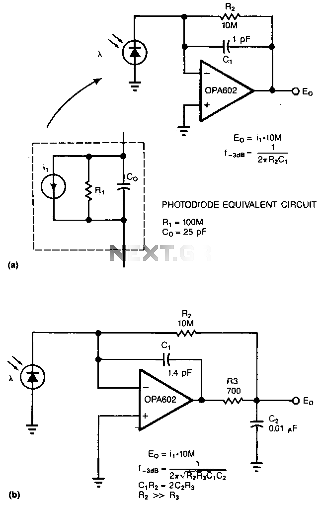
Adding two passive components to a standard photodiode amplifier reduces noise. Without the modification, the shunt capacitance of the photodiode reacting with the relatively large feedback resistor of the transimpedance (current-to-voltage) amplifier creates excessive noise gain. The improved circuit adds a second pole, formed by R3 and C2. The modifications reduce noise by a factor of 3. Because the pole is within the feedback loop, the amplifier maintains its low output impedance. If the pole is placed outside the feedback loop, an additional buffer must be added, which would increase noise and error. The signal bandwidth of both circuits is 16 kHz. In the standard circuit, the 1-pF stray capacitance in the feedback loop forms a single 16-kHz pole. The improved circuit has the same bandwidth as the first but exhibits a 2-pole response.
The enhancement of a standard photodiode amplifier's performance is achieved through the integration of two passive components, specifically a resistor (R3) and a capacitor (C2). This modification effectively addresses the issue of excessive noise gain that arises from the interaction between the photodiode's shunt capacitance and the feedback resistor within the transimpedance amplifier configuration. By introducing a second pole into the circuit, the noise level is significantly reduced, achieving a noise reduction factor of three.
In the original configuration, the circuit is limited by the presence of a single pole formed by the 1-pF stray capacitance in the feedback loop, which results in a bandwidth of 16 kHz. The introduction of the second pole, however, allows for a more complex frequency response while maintaining the same bandwidth. This is crucial as it enables the amplifier to preserve its low output impedance, which is an essential characteristic for ensuring signal integrity and minimizing distortion.
It is important to note that positioning the additional pole outside the feedback loop would necessitate the inclusion of a buffer stage. This alteration would inadvertently introduce additional noise and potential error into the system, counteracting the benefits gained from the initial modification. Therefore, the improved design maintains the pole within the feedback loop, ensuring optimal performance and reduced noise levels.
The schematic representation of the modified circuit (referenced as Fig. 3-18b) would illustrate the arrangement of the components, highlighting the feedback loop and the placement of R3 and C2. The design's effectiveness is underscored by the enhanced stability and reduced noise characteristics while maintaining the required signal bandwidth of 16 kHz. This approach exemplifies a practical solution in the field of electronic circuit design, specifically in applications requiring high precision and low noise in photodiode amplification.Adding two passive components to a standard photodiode amplifier reduces noise. Without the modification, the shunt capacitance of the photodiode reacting with the relatively large feedback resistor of the transimpedance (current-to-voltage) amplifier, creates excessive noise gain. The improved circuit, Fig. 3-18b, adds a second pole, formed by R3 and C2. The modifications reduce noise by a factor of 3. Because the pole is within the feedback loop, the amplifier maintains its low output impedance. If you place the pole outside the feedback loop, you have to add an additional buffer, which would increase noise and de error. The signal bandwidth of both circuits is 16kHz. In the standard circuit (Fig. 3-18a), the 1-pF stray capacitance in the feedback loop forms a single 16-kHz pole. The improved circuit has the same bandwidth as the first, but exhibits a 2-pole response. 🔗 External reference
Related Circuits
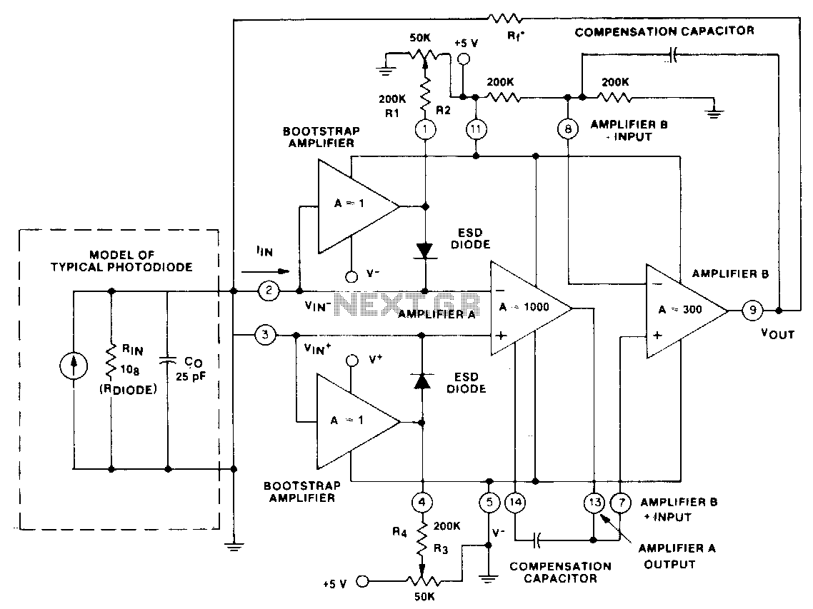
This circuit utilizes a CA5422 dual BiMOS microprocessor operational amplifier. The bootstrap amplifiers reduce bias currents while providing electrostatic discharge protection. Additionally, the potentiometers and their corresponding resistors, R1 through R4, allow the user to adjust bias currents to...