PIC Microcontroller
1. Architecture and Core Features
PIC Microcontroller Architecture and Core Features
Harvard Architecture Implementation
The PIC microcontroller family employs a modified Harvard architecture, characterized by separate buses for instruction and data memory. This design enables simultaneous instruction fetching and data access, eliminating von Neumann bottlenecks. The program memory bus typically operates at 12, 14, or 16 bits width (depending on PIC family), while the data memory bus maintains an 8-bit width. Advanced variants implement pipeline execution, allowing single-cycle instruction execution (excluding branches) at clock speeds up to 200 MHz in modern PIC32MX/MZ series.
Register File Structure
The Working Register (WREG) serves as the primary accumulator, with additional Special Function Registers (SFRs) mapped across all memory banks. The register file organization follows:
Bank switching occurs through the STATUS register's RP bits (in baseline models) or BSR register (in enhanced mid-range cores). Peripheral control registers are memory-mapped, enabling uniform access through MOVF and MOVWF instructions.
Instruction Set Characteristics
PIC microcontrollers utilize a RISC-based instruction set with fixed-length encoding. The baseline series (PIC10/12/16) implements 33 instructions, while enhanced cores (PIC18) extend this to 75 instructions. Key features include:
- Single-cycle ALU operations (ADDWF, ANDWF)
- Bit-oriented operations (BSF, BCF) with 1-cycle execution
- Hardware stack with depth varying by model (2-31 levels)
- Relative branching with 8-bit offset (BRA instruction)
Clock Generation and Power Management
Modern PIC devices incorporate multiple clock domains with flexible source selection:
The Power-up Timer (PWRT) and Oscillator Start-up Timer (OST) ensure stable operation during wake-up from sleep modes, which typically consume <1 μA. Clock switching permits dynamic performance scaling through the OSCCON register.
Peripheral Integration
Advanced PIC models incorporate:
- 12-bit ADCs with hardware threshold detection (CTMU in PIC24F)
- Configurable Logic Cells (CLC) for hardware-based state machines
- Direct Memory Access (DMA) controllers with peripheral-to-memory routing
- Hardware crypto engines (AES/SHA in PIC32MZ)
Memory Technologies
Flash memory endurance follows the Arrhenius model:
Where Ea ≈ 0.6 eV for PIC flash cells. Data EEPROM provides 1M erase/write cycles with byte-level granularity. Advanced models implement Error Correction Codes (ECC) for program memory.
1.2 Memory Organization
Memory Architecture Overview
The PIC microcontroller employs a Harvard architecture, distinguishing it from von Neumann architectures by separating program and data memory spaces. This design allows simultaneous access to instruction and data buses, significantly improving throughput. The memory organization is hierarchical, consisting of:
- Program Memory (Flash/ROM): Stores firmware and executable code, typically non-volatile.
- Data Memory (RAM): Volatile storage for runtime variables and stack operations.
- EEPROM: Non-volatile memory for persistent data storage.
- Special Function Registers (SFRs): Control peripheral and core functionalities.
Program Memory Structure
Program memory is organized into words, where each word corresponds to a 12-bit, 14-bit, or 16-bit instruction, depending on the PIC family (e.g., PIC10/12, PIC16, PIC18). The memory is linearly addressable, with the reset vector located at the highest address (e.g., 0x0000 for mid-range PICs). Interrupt vectors occupy fixed locations, such as 0x0004 in PIC16F series.
where n is the width of the program counter (e.g., 13 bits in PIC16F877A, yielding 8K words).
Data Memory and Banking
Data memory is partitioned into banks, each 128 bytes wide, accessed via the STATUS register's RP0 and RP1 bits. For example, PIC16F877A uses four banks (Bank 0–3), with SFRs mirrored across banks for efficiency. Direct addressing is limited to the current bank, while indirect addressing via the FSR and INDF registers bypasses this constraint.
Special Function Registers (SFRs)
SFRs control core features (e.g., STATUS, PCLATH) and peripherals (e.g., PORTA, TMR0). Their addresses are fixed, with critical registers like STATUS at 0x03 (Bank 0) and 0x83 (Bank 1).
EEPROM and Access Methods
EEPROM provides non-volatile storage with byte-level granularity. Access involves:
- Writing the address to
EEADRand data toEEDATA. - Configuring
EECON1(e.g.,WREN=1to enable writes). - Executing a timed write sequence to prevent accidental corruption.
Memory-Mapped Peripherals
Peripherals like ADCs and timers are memory-mapped into data space. For instance, the PIC16F877A's ADC result registers (ADRESH/ADRESL) reside at 0x1E and 0x1F in Bank 0.
Practical Considerations
Bank switching overhead can degrade performance in time-critical applications. Optimizations include:
- Placing frequently accessed variables in shared memory regions (e.g., Bank 0).
- Using indirect addressing for cross-bank data manipulation.
- Leveraging compiler directives (e.g.,
__section) for memory placement.
1.3 Instruction Set and Execution Pipeline
Instruction Set Architecture (ISA) Overview
The PIC microcontroller employs a RISC-based instruction set, optimized for single-cycle execution (excluding branches). The ISA is classified as Harvard architecture, featuring separate program and data buses. Key characteristics include:
- Fixed-length instructions (12/14/16 bits depending on PIC family)
- Orthogonal register set with WREG as the working register
- Single-cycle ALU operations (ADDWF, ANDLW, etc.)
- Two-phase clocking system for pipelined execution
Pipeline Structure and Timing
The PIC uses a two-stage fetch-execute pipeline:
where Tosc is the oscillator period. The pipeline stages are:
- Fetch: Instruction read from program memory
- Execute: Decode and operation execution
This creates an effective single-cycle execution for most instructions, with the following timing relationship:
where Pbranch represents the probability of pipeline stalls due to branches.
Instruction Categories
1. Byte-Oriented Operations
Format: OPCODE f,d where f is file register address and d selects destination (WREG or f). Example:
ADDWF REG1,0 ; WREG ← WREG + REG12. Bit-Oriented Operations
Format: OPCODE f,b where b is the bit position (0-7). Example:
BSF STATUS,C ; Set Carry flag3. Literal Operations
Format: OPCODE k where k is an 8-bit constant. Example:
MOVLW 0x3A ; WREG ← 0x3A4. Control Operations
Includes branches, calls, and returns. These require two cycles due to pipeline flushing:
CALL SUBROUTINE ; 2-cycle operationPipeline Hazards and Mitigation
The PIC architecture exhibits two primary hazards:
- Structural hazards: Resolved via Harvard architecture separation
- Control hazards: Branches incur 1-cycle penalty
Data hazards are minimized through:
where tsetup accounts for register file access timing constraints.
Real-World Performance Considerations
In practical applications, the following factors affect pipeline efficiency:
- Interrupt service routines (2-cycle latency)
- Data table reads (disrupts pipeline flow)
- Sleep mode wake-up delays
The effective MIPS rating can be calculated as:
where α represents the fraction of branch/jump instructions.
2. Integrated Development Environments (IDEs)
2.1 Integrated Development Environments (IDEs)
Developing firmware for PIC microcontrollers requires a robust Integrated Development Environment (IDE) that integrates code editing, compilation, debugging, and device programming. The choice of IDE significantly impacts development efficiency, debugging capabilities, and hardware compatibility.
MPLAB X IDE
Microchip's MPLAB X IDE is the official development platform for PIC microcontrollers, built on NetBeans for cross-platform support (Windows, Linux, macOS). Key features include:
- Seamless integration with XC compilers (XC8, XC16, XC32) for 8-bit, 16-bit, and 32-bit PIC MCUs
- Advanced debugging via MPLAB ICE and PICKit programmers
- Static code analysis and version control (Git, SVN) integration
where CPI (cycles per instruction) depends on the PIC architecture (e.g., ~4 for baseline PICs, ~1.3 for PIC18 with hardware multiplier).
Third-Party Alternatives
While MPLAB X dominates, alternatives offer specialized advantages:
MikroC PRO for PIC
Notable for its rich hardware library and rapid prototyping tools:
- One-click peripheral initialization (UART, SPI, PWM)
- Built-in hardware abstraction layers (HAL) for common sensors
- Real-time code metrics (ROM/RAM usage, execution cycles)
CCS C Compiler
Optimized for deterministic timing in control systems:
- Cycle-accurate simulation for critical loops
- Direct hardware register access through #use directives
- Smaller code footprint compared to XC8 in some benchmarks
Debugging Architectures
Modern PIC IDEs implement two-tier debugging:
- Software Emulation: MPLAB SIM simulates instruction flow without hardware
- Hardware Debugging: ICD4/Real ICE supports breakpoints, trace, and live variable monitoring
Debug probe bandwidth (B) must satisfy:
where fdebug is the debug clock frequency (typically 1/4 of fCPU).
Cloud-Based Development
MPLAB Xpress and MPLAB Cloud introduce browser-based workflows:
- Automatic toolchain updates (no local installation)
- Collaborative project sharing with access control
- Secure OTA firmware updates through cloud programmers
2.2 Compilers and Assemblers
Compiler vs. Assembler: Fundamental Differences
Compilers and assemblers serve distinct roles in microcontroller programming. A compiler translates high-level language code (e.g., C, C++) into machine-readable instructions, optimizing for memory and speed. In contrast, an assembler converts assembly language (mnemonics like MOVLW, ADDWF) directly into binary opcodes. While compilers abstract hardware details, assemblers provide granular control over PIC registers and timing-critical operations.
PIC-Specific Toolchains
For PIC microcontrollers, the dominant compiler suites include:
- MPLAB XC Compilers (XC8, XC16, XC32) — Optimized for 8-bit, 16-bit, and 32-bit PIC MCUs, with free and paid tiers offering varying optimization levels.
- CCS C Compiler — Supports inline assembly and hardware-specific libraries for rapid development.
- SDCC (Small Device C Compiler) — Open-source, targeting PIC16/18 architectures with moderate optimization.
Assemblers like MPASM (Microchip’s legacy tool) and GPASM (part of the open-source gputils suite) parse assembly directives such as ORG and END while resolving labels and macros.
Optimization Techniques in Compilation
Compiler optimizations for PIC devices focus on:
- Peephole Optimization — Replaces inefficient instruction sequences (e.g., redundant
MOVFoperations) with shorter equivalents. - Register Allocation — Minimizes access to slow RAM by prioritizing WREG and STATUS registers.
- Loop Unrolling — Trade-off between speed and memory by expanding loops statically.
Inline Assembly for Critical Sections
When timing precision is paramount (e.g., ISRs or bit-banged protocols), inline assembly embeds low-level instructions within high-level code. Example for a PIC16F877A delay loop:
void delay_1ms() {
  __asm(
    "MOVLW 0xFF  \n\t"
    "MOVWF _count \n\t"
    "LOOP: DECFSZ _count, F \n\t"
    "GOTO LOOP    \n\t"
  );
}
Debugging and Output Analysis
Compiler-generated .lst and .map files dissect memory usage and instruction flow. For assemblers, the .hex file’s address-data pairs verify correctness against the PIC’s program memory layout. Logic analyzers or MPLAB’s simulator correlate machine cycles with source lines.
Case Study: Compiler Efficiency Comparison
A benchmark of XC8 (free vs. Pro) for a 256-byte AES implementation on a PIC18F45K22 revealed:
- Free Mode: 1,842 bytes (no optimization).
- Pro Mode (-O3): 1,214 bytes (25% smaller, 18% faster).
Such trade-offs guide toolchain selection for resource-constrained applications.
2.3 Debugging and Simulation Tools
In-Circuit Debuggers (ICD)
In-circuit debuggers, such as PICkit 4 and MPLAB ICD 4, provide real-time execution control and register inspection while the microcontroller operates in its target environment. These tools interface with the Debug Executive firmware, which is programmed into a reserved portion of the PIC's memory. The debugger communicates via the In-Circuit Serial Programming (ICSP) interface, allowing breakpoint insertion, single-stepping, and watch variable monitoring without disrupting peripheral functionality.
Hardware Simulation with MPLAB X IDE
MPLAB X IDE integrates a cycle-accurate simulator that models PIC microcontroller behavior at the instruction level. The simulator supports:
- Peripheral register emulation with full bit-field resolution
- Interrupt latency calculation with pipeline effects
- Power consumption estimation based on activity profiles
For timing-critical applications, the simulator's clock tree model accounts for oscillator startup delays, PLL lock times, and clock domain crossing hazards.
Real-Time Trace Capture
Advanced debuggers like MPLAB REAL ICE implement instruction trace buffers using on-chip debug modules or external trace ports. The trace data follows the execution flow with nanosecond resolution, enabling:
where τtrace represents the exact timing deviation from ideal execution. Trace visualization tools correlate program counter movements with peripheral events and data bus transactions.
Mixed-Signal Simulation
When integrating analog front-ends, MPLAB Mindi analog simulator couples with digital models through:
- SPICE-level accuracy for continuous-time signals
- Event-driven simulation for digital peripherals
- Mixed-signal breakpoints triggering on voltage thresholds
The co-simulation interface resolves analog-to-digital conversion artifacts, including quantization noise and aperture jitter.
Fault Injection Testing
Debug tools support deliberate fault scenarios to validate error handling routines:
where λ represents the fault injection rate. Test cases include register corruption, clock glitches, and power supply transients. The Hardware Abstraction Layer (HAL) provides hooks for fault detection mechanisms.
Performance Profiling
Statistical profilers in MPLAB X measure:
- Worst-case execution time (WCET) through path analysis
- Cache hit/miss ratios for Harvard architecture variants
- Interrupt service routine (ISR) latency distributions
The profiler generates execution heatmaps overlayed on disassembled code, identifying optimization bottlenecks.
Automated Verification Frameworks
Formal verification tools like MPLAB Code Coverage apply model checking to ensure:
- Branch coverage meets safety-critical standards (e.g., IEC 61508)
- All peripheral configurations are exercised
- Defensive programming constructs are triggered
The framework generates test vectors that achieve 100% modified condition/decision coverage (MC/DC) for certification.
// Example debug configuration for XC8 compiler
#pragma config DEBUG = ON       // Enable debug mode
#pragma config ICS = PGD2       // Dedicated debug port
#pragma config JTAGEN = OFF     // Disable JTAG for debug pins

void __attribute__((debug)) critical_function() {
    asm("MOV #SFRBASE, W0");   // Inline assembly visible in debugger
    INTCON1bits.NSTDIS = 1;     // Enable nested interrupt debugging
}
3. Writing and Compiling Code
3.1 Writing and Compiling Code
Development Environment Setup
To begin writing code for PIC microcontrollers, an Integrated Development Environment (IDE) such as MPLAB X or Microchip Studio is essential. These IDEs provide a comprehensive suite of tools, including:
- Code editor with syntax highlighting
- Project management
- Compiler toolchain integration (XC8, XC16, or XC32)
- Debugging and simulation capabilities
Installation involves downloading the IDE from Microchip’s official website, along with the appropriate compiler for the target PIC architecture (8-bit, 16-bit, or 32-bit).
Writing Firmware in C
PIC microcontrollers are commonly programmed in C due to its efficiency and hardware-level control. A basic firmware structure includes:
- Configuration bits setup (e.g., oscillator selection, watchdog timer)
- Peripheral initialization (e.g., GPIO, UART, ADC)
- Main application loop
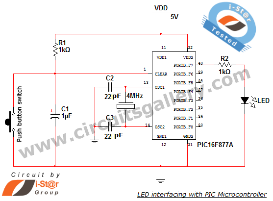
Below is an example of a simple LED blink program for a PIC16F877A:
#include <xc.h>
#pragma config FOSC = HS      // High-speed oscillator
#pragma config WDTE = OFF     // Watchdog Timer disabled

void main() {
    TRISB0 = 0;              // Set RB0 as output
    while(1) {
        RB0 = 1;             // LED ON
        __delay_ms(500);     // 500ms delay
        RB0 = 0;             // LED OFF
        __delay_ms(500);     // 500ms delay
    }
}
Compiler Toolchain and Optimization
The XC8 compiler (for 8-bit PICs) translates C code into machine-readable hex files. Key compiler optimizations include:
- Speed vs. Size Trade-offs:
-O1(balanced),-O3(aggressive speed optimization) - Debug Symbols:
-gfor debugging - Processor-Specific Tuning:
-mcpu=16f877a
Compiler directives such as #pragma are used to configure hardware-specific settings (e.g., oscillator mode, reset behavior).
Linking and Memory Allocation
The linker script (.lkr file) defines memory regions (program Flash, RAM, EEPROM) and assigns sections:
.textfor executable code.datafor initialized variables.bssfor uninitialized variables
Memory constraints on PIC devices require careful management. For example, bank switching may be necessary for larger variables.
Building and Output Files
Compilation generates several output files:
- .hex: Intel HEX format for programming
- .cof: Debugging information
- .map: Memory usage report
To compile from the command line (e.g., for CI/CD pipelines):
xc8 --chip=16f877a --outdir=build main.c
Debugging and Simulation
MPLAB X integrates with hardware debuggers (e.g., PICkit 4 or ICD 4) for real-time debugging. Breakpoints, watch variables, and register inspection are supported. For simulation, the MPLAB SIM tool emulates peripheral behavior without hardware.
Real-World Considerations
Advanced applications (e.g., motor control, DSP) often require:
- Inline assembly for timing-critical sections
- Interrupt Service Routines (ISRs) with low latency
- Power consumption optimization via sleep modes
3.2 Interfacing with Peripherals
GPIO Configuration and Electrical Characteristics
PIC microcontrollers feature General-Purpose Input/Output (GPIO) pins that can be dynamically configured for digital input or output. Each pin is associated with three primary registers:
- TRISx (Data Direction Register): Determines whether a pin is input (1) or output (0).
- PORTx (Reads the current state of the pin).
- LATx (Latch Register): Writes output values to the pin.
The electrical characteristics of GPIO pins are governed by the microcontroller's datasheet. For a PIC16F877A operating at 5V:
Analog-to-Digital Conversion (ADC)
The ADC module in PIC microcontrollers converts analog signals to digital values with configurable resolution (typically 8–12 bits). The conversion process follows:
- Configure the ADC module using ADCON0 and ADCON1 registers.
- Set the acquisition time to ensure proper sampling:
Where \( T_{AD} \) is the ADC clock period. The digital output is derived as:
PWM Generation
Pulse-Width Modulation (PWM) is achieved using the CCP (Capture/Compare/PWM) module. The duty cycle and frequency are calculated as:
Serial Communication (UART, SPI, I2C)
PIC microcontrollers support multiple serial protocols:
- UART: Asynchronous communication with configurable baud rate via the TXREG and RCREG registers.
- SPI: Full-duplex communication using SS, SCK, MOSI, and MISO pins.
- I2C: Two-wire interface with clock stretching support.
Interrupt Handling
Peripheral interrupts are managed via the INTCON and PIRx registers. Interrupt Service Routines (ISRs) must:
- Clear the interrupt flag.
- Preserve context (e.g., saving WREG and STATUS registers).
// Example: Configuring UART on PIC16F877A
void UART_Init() {
    TXSTA = 0x24;   // Enable TX, 8-bit mode, async mode
    RCSTA = 0x90;   // Enable serial port, continuous receive
    SPBRG = 25;     // 9600 baud @ 4MHz clock
}
3.3 Interrupt Handling and Timers
Interrupt Architecture in PIC Microcontrollers
Interrupts in PIC microcontrollers are hardware-triggered events that temporarily halt the normal program flow to execute an Interrupt Service Routine (ISR). The PIC architecture supports multiple interrupt sources, including:
- Timer overflow (TMR0, TMR1, TMR2)
- External interrupts (INT0, INT1, INT2)
- Analog-to-Digital Converter (ADC) completion
- Serial communication events (UART, SPI, I²C)
Each interrupt source has an associated flag bit (e.g., TMR0IF for Timer0) in the INTCON or PIR registers and an enable bit (e.g., TMR0IE) to activate the interrupt. The Global Interrupt Enable (GIE) bit in the INTCON register must be set to allow any interrupts to trigger.
Interrupt Priority and Vectoring
Advanced PIC microcontrollers (e.g., PIC18F series) support interrupt prioritization. Two priority levels—high and low—are managed via the IPR (Interrupt Priority Register) and RCON.IPEN (Interrupt Priority Enable) bits. The ISR for high-priority interrupts is located at address 0x0008, while low-priority ISRs reside at 0x0018.
where \(N_{cycles}\) is the number of clock cycles required to complete the current instruction and \(T_{clock}\) is the clock period. Minimizing latency is critical for real-time applications.
Timer Modules: Operational Modes
PIC microcontrollers integrate multiple timer modules, each configurable for specific timing tasks:
Timer0 (8/16-bit)
Timer0 can operate as an 8-bit or 16-bit counter with a prescaler (1:1 to 1:256). The overflow rate is calculated as:
where \(n\) is the timer bit-width (8 or 16), and TMR0 is the initial value loaded into the timer register.
Timer1 (16-bit with Gate Control)
Timer1 includes a gate control feature, allowing external signals to enable/disable counting. It is often used for:
- Pulse-width measurement
- Frequency counting in conjunction with the Capture/Compare/PWM (CCP) module
Timer2 (8-bit with PWM)
Timer2 is tailored for PWM generation, featuring a postscaler and period register (PR2). The PWM period is given by:
Practical Implementation: Interrupt-Driven Timer
Below is an example of configuring Timer0 for a 1ms interrupt on a PIC18F4550 (16 MHz clock):
#include <xc.h>
void __interrupt() ISR(void) {
    if (TMR0IF) {
        TMR0IF = 0;     // Clear interrupt flag
        TMR0 = 3036;    // Reload for 1ms (16MHz, prescaler 1:8)
        // User code here
    }
}
void main() {
    T0CON = 0xC2;       // Timer0 ON, 16-bit, prescaler 1:8
    TMR0 = 3036;        // Initial value for 1ms
    INTCON = 0xE0;      // Enable Timer0 and global interrupts
    while(1);
}
Applications and Optimization
Interrupt-driven timers are essential for:
- Real-time systems: Task scheduling in RTOS.
- Sensor polling: Periodic ADC sampling.
- Communication protocols: UART baud rate generation.
To reduce jitter, avoid long ISRs and use hardware-assisted PWM or CCP modules for timing-critical signals.
4. Sensor Interfacing and Data Acquisition
4.1 Sensor Interfacing and Data Acquisition
Sensor Signal Conditioning
Most sensors output analog signals with non-linearities, noise, or weak amplitudes. A PIC microcontroller's ADC requires a conditioned signal within its reference voltage range (typically 0–5V). Key conditioning stages include:
- Amplification: Op-amps (e.g., MCP6002) scale millivolt-level signals (e.g., thermocouples) to the ADC's input range. Gain is set by resistor ratios:
$$ G = 1 + \frac{R_f}{R_{in}} $$
- Filtering: Passive RC or active filters (Butterworth, Bessel) attenuate high-frequency noise. For a cutoff frequency \( f_c \):
$$ f_c = \frac{1}{2\pi RC} $$
- Impedance Matching: Voltage followers (unity-gain buffers) prevent signal degradation when interfacing high-impedance sensors (e.g., pH probes).
ADC Configuration and Sampling
PIC microcontrollers integrate 10–12 bit ADCs with configurable acquisition times and reference voltages. Critical parameters include:
- Clock Source: Derived from the system clock (Fosc/2 to Fosc/32) to meet the ADC's TAD requirement (e.g., 1.6 µs for PIC16F877A).
- Channel Selection: Multiplexed inputs (AN0–ANx) require software-controlled switching and settling delays.
- Sampling Rate: Limited by conversion time (Tconv = TAD × (bits + 1)). For a 10-bit ADC at 4 MHz Fosc:
$$ T_{conv} = 12 \times \left(\frac{1}{4 \text{MHz}/2}\right) = 6 \mu\text{s} $$
Digital Communication Protocols
For digital sensors (I2C, SPI, UART), PICs implement hardware peripherals or bit-banged software protocols. Key considerations:
- I2C: 7/10-bit addressing, pull-up resistors (1–10 kΩ), and clock stretching (for slow slaves).
- SPI: Configurable clock polarity (CPOL) and phase (CPHA) to match sensor requirements.
- Error Handling: CRC checks (for UART), ACK/NACK verification (I2C), and timeout mechanisms.
Real-World Case: LM35 Temperature Sensor
The LM35 outputs 10 mV/°C with ±0.5°C accuracy. Interfacing with a PIC16F877A involves:
- Direct connection to AN0 (no amplification needed for 0–150°C range).
- ADC configured for VREF+ = 5V, right-justified result, and Fosc/8 clock.
- Temperature calculation:
$$ T = \frac{ADC \times 500}{1023} $$
Noise Mitigation Techniques
High-resolution measurements require:
- Averaging: Oversampling and decimation improve ENOB (Effective Number of Bits).
- Shielding: Twisted-pair cables for analog signals reduce EMI pickup.
- Grounding: Star topology separates analog and digital grounds, connected at a single point.
Dynamic Range Optimization
For sensors with wide output ranges (e.g., 0–50 mV to 0–5V), programmable gain amplifiers (PGAs) or auto-ranging circuits adapt the ADC's resolution to the signal's amplitude. A digital potentiometer (e.g., MCP4131) can adjust gain dynamically via SPI.
4.2 Motor Control and Robotics
PWM-Based Motor Speed Control
Precision motor control in robotics relies heavily on Pulse-Width Modulation (PWM) generated by PIC microcontrollers. The duty cycle (D) of the PWM signal determines the average voltage applied to the motor, given by:
For brushed DC motors, the relationship between PWM frequency (fPWM) and torque ripple is critical. A higher frequency reduces audible noise but increases switching losses. The optimal range for most robotics applications lies between 5–20 kHz. PIC microcontrollers with Enhanced PWM (EPWM) modules, such as the PIC18F45K22, allow dead-time insertion to prevent shoot-through in H-bridge configurations.
Closed-Loop Control Systems
Robotic systems often implement PID control for precise motion regulation. The PIC’s analog-to-digital converter (ADC) samples feedback from encoders or current sensors, while the PID algorithm computes corrective actions. The discrete-time PID equation implemented in firmware is:
where u[k] is the control output, e[k] is the error signal, and Δt is the sampling period. Anti-windup techniques must be applied to prevent integral term saturation during prolonged errors.
H-Bridge Circuit Design
Bidirectional motor control requires an H-bridge, typically built with MOSFETs or motor driver ICs like the L298N. The PIC’s GPIO pins drive the bridge’s input logic, with strict attention to:
- Dead-time insertion (≥1 μs) to prevent cross-conduction
- Opto-isolation for high-voltage (>24V) applications
- Flyback diodes (Schottky or TVS) for inductive kickback protection
Stepper Motor Microstepping
For precision robotics, PIC-driven stepper motors often use microstepping to reduce vibration. A sine-cosine PWM profile divides full steps into smaller increments. The current per phase (IA, IB) follows:
where θ is the electrical angle. PIC16F1789 devices with Complementary Waveform Generator (CWG) modules simplify this implementation.
Real-World Implementation: Robotic Arm Joint Control
A 6-DOF robotic arm joint demonstrates these principles. The PIC18F46K42:
- Generates 4-phase PWM signals for two NEMA 17 steppers
- Samples quadrature encoders via the Input Capture module
- Implements torque control using ADC readings from INA240 current sensors
// PIC18F46K42 PWM initialization for motor control
void PWM_Init() {
  PR2 = 199;          // 20 kHz PWM @ 64 MHz Fosc
  CCP1CON = 0x0C;     // PWM mode, active-high
  CCPR1L = 0;         // Initial duty cycle = 0%
  T2CON = 0x04;       // Timer2 on, prescaler 1:1
  TRISCbits.TRISC2 = 0; // CCP1 output enable
}
4.3 Communication Protocols (UART, SPI, I2C)
Universal Asynchronous Receiver-Transmitter (UART)
The UART protocol provides full-duplex serial communication using two wires (TX and RX) without a clock signal. Data transmission follows an asynchronous frame structure:
- Start bit (logic low)
- 5-9 data bits (LSB first)
- Optional parity bit (even, odd, or none)
- 1-2 stop bits (logic high)
The baud rate must match between transmitter and receiver, with allowable error typically below 2%. The PIC microcontroller's UART module calculates the baud rate generator value using:
Where BRGH selects high/low speed mode. Advanced implementations use auto-baud detection and hardware flow control (RTS/CTS) for reliable high-speed communication.
Serial Peripheral Interface (SPI)
SPI operates in full-duplex synchronous mode using four signals:
- SCK (Serial Clock)
- MOSI (Master Out Slave In)
- MISO (Master In Slave Out)
- SS (Slave Select)
The PIC microcontroller's SPI module supports multiple modes determined by clock polarity (CPOL) and phase (CPHA):
| Mode | CPOL | CPHA |
|---|---|---|
| 0 | 0 | 0 |
| 1 | 0 | 1 |
| 2 | 1 | 0 |
| 3 | 1 | 1 |
The maximum SPI clock frequency is Fosc/4 in master mode. For high-speed data acquisition systems, the PIC's SPI interface can achieve 10+ Mbps with DMA support.
Inter-Integrated Circuit (I²C)
I²C is a multi-master, multi-slave protocol using two wires (SDA and SCL) with open-drain outputs. The PIC microcontroller implements I²C with:
- 7-bit or 10-bit addressing
- Standard (100 kHz) and Fast (400 kHz) modes
- Clock stretching support
The I²C baud rate generator uses:
Advanced features include:
- Bus collision detection
- Software-controlled clock stretching
- Multi-byte transmission with automatic ACK/NACK handling
In high-noise environments, the Schmitt trigger inputs and programmable noise filters improve reliability. The I²C module supports SMBus protocols with timeout detection and alert responses.
Protocol Selection Criteria
When implementing communication in PIC-based systems:
- UART is optimal for point-to-point communication over longer distances
- SPI provides highest throughput for short-distance chip-to-chip communication
- I²C is preferred for multi-device systems with limited pins
Modern PIC microcontrollers integrate enhanced versions of these protocols, such as EUSART (with LIN support), SPI with FIFO buffers, and I²C with SMBus 3.0 compatibility.
5. Official Documentation and Datasheets
5.1 Official Documentation and Datasheets
- PDF PIC1000: Getting Started with Writing C-Code for PIC16 and PIC18 — 1. Data Sheet Module Structure and Naming Conventions The first step in writing C-code for a microcontroller is knowing and understanding the type of information found in the data sheet of the device used for programming. The data sheet contains information about the features, memories, core and peripheral modules of the microcontroller.
- Development Tools Listing | Microchip Technology — PIC® MCUs; AVR® Microcontrollers (MCUs) 16-bit MCUs; View All; PIC24F GU/GL/GP MCUs; PIC24F GA MCUs; PIC24F GB MCUs; PIC24F GC MCUs; Digital Signal Controllers (DSCs) View All; dsPIC33A DSCs; dsPIC33C DSCs; dsPIC33E DSCs; Integrated Motor Drivers With dsPIC DSCs; 32-bit MCUs; View All; PIC32A High-Performance MCUs; PIC32C Arm® Cortex®-Based ...
- PDF PIC16C505 Data Sheet - Microchip Technology — Device included in this Data Sheet: PIC16C505 High-Performance RISC CPU: • Only 33 instructions to learn † Operating speed: - DC - 20 MHz clock input - DC - 200 ns instruction cycle † Direct, indirect and relative addressing modes for data and instructions † 12-bit wide instructions † 8-bit wide data path † 2-level deep hardware stack
- PIC® Microcontrollers (MCUs) | Microchip Technology — PIC ® Microcontrollers (MCUs) Achieve new levels of capability and performance with the easy-to-use and robust design of PIC® MCUs. Their integrated peripherals provide outstanding efficiency and flexibility, making them an excellent choice for low-power compact designs and high-performance applications such as smartphones, audio accessories ...
- A Guide To PIC Microcontroller Documentation - Wikibooks — A PIC microcontroller. Datasheets for semiconductor products can be baffling even for the most experienced engineers and programmers, but those written for microcontroller or digital signal processing products are even more so. One of the challenges of writing a datasheet for such products is that, due to their programmable nature, diversity ...
- A Guide To PIC Microcontroller Documentation/Print version — In this section we will be taking an in depth look at the main documentation for one controller out of each PIC microcontroller family. In each case the key documents will be listed and then the datasheet will be analysed chapter by chapter to highlight the information that is provided, and how related information can be found in the cases ...
- A Guide To PIC Microcontroller Documentation/Documentation structure ... — Documentation for microcontroller and DSC products can be broken down into three core document types: Datasheet - the datasheet documents how a specific controller device, or a group of devices with the same subset of features, functions. This document typically includes, as a minimum, descriptions of the processing core, memory, peripherals, electrical characteristics, timing characteristics ...
- PDF 8-bit PIC Microcontroller Peripheral Integration - Microchip Technology — 8-bit PIC® Microcontrollers Product Family Pin Count Program Flash Memory (KB) RAM (KB) Data EE (B) Intelligent Analog Waveform Control Logic and Math Safety and Monitoring Communications User Interface Low Power and System Flexibility
- PIC Controllers - ElectronicWings — PIC is a microcontroller family developed by Microchip Technology and has a wide range of uses in embedded systems. + Project. ... Serial Peripheral Interface (SPI) is a communication protocol used by the microcontroller for communicating with one or more devices serially over short distance. It is used to communicate with devices like SD card ...
- PDF 8-Pin PICmicro® Microcontroller Family Product Information — an electronic design. Now, designers can implement the same, or even more functionality into an 8-pin microcontroller that is cost competitive and uses less board space. In addition, the designer gains the flexibility to add new features on a regular basis or adapt the design to changing requirements without hardware changes.
5.2 Recommended Books and Guides
- PIC microcontrollers : an introduction to microelectronics : Bates ... — Access-restricted-item true Addeddate 2022-12-12 23:01:56 Associated-names Bates, Martin, 1952- Introduction to microelectronic systems Autocrop_version ..14_books-20220331-.2 Boxid IA40790905 Camera Sony Alpha-A6300 (Control) Collection_set printdisabled External-identifier urn:lcp:picmicrocontroll0000bate_r9y1:epub:8b083ecf-4411-414c-aa96-e3d76749f0b9 urn:lcp:picmicrocontroll0000bate_r9y1 ...
- PDF PIC1000: Getting Started with Writing C-Code for PIC16 and PIC18 — This technical brief provides the steps recommended to successfully program a PIC16 or PIC18 microcontroller and defines coding guidelines to help write more readable and reusable code.
- PIC Projects: A Practical Approach | Wiley — This book is a collection of projects based around various microcontrollers from the PIC family. The reader is carefully guided through the book, from very simple to more complex projects in order to gradually build their knowledge about PIC microcontrollers and digital electronics in general. On completion of this book, the reader should be able to design and build their own projects and ...
- PDF Microsoft Word - 5.2.1 PIC Microcontrollers - WJEC — A complication - PIC microcontrollers are an extensive and important group of microcontrollers, present in a wide range of devices from DVD players to engine management systems.
- Programming the PIC Microcontroller with MBASIC (Embedded Technology) — The Microchip PIC family of microcontrollers is the most popular series of microcontrollers in the world. However, no microcontroller is of any use without software to make it perform useful functions. This comprehensive reference focuses on designing with Microchip's mid-range PIC line using MBASIC, a powerful but easy to learn programming language. It illustrates MBASIC's abilities ...
- PDF Advanced PIC Microcontroller Projects in C — Recognizing the importance of preserving what has been written, Elsevier prints its books on acid-free paper whenever possible. Library of Congress Cataloging-in-Publication Data Ibrahim, Dogan. Advanced PIC microcontroller projects in C: from USB to RTOS with the PIC18F series/Dogan Ibrahim p. cm. Includes bibliographical references and index.
- Designing embedded systems with PIC microcontrollers : principles and ... — This book takes the novice from introduction of embedded systems through to advanced development techniques for utilizing and optimizing the PIC family of microcontrollers in your device.
- Easy PIC'n : a beginner's guide to using PIC16/17 microcontrollers from ... — Easy PIC'n : a beginner's guide to using PIC16/17 microcontrollers from square 1 by Benson, David
- PDF Programming 8-bit Pic Microcontrollers in C — Martin Bates, best-selling author, has provided a step-by-step guide to programming these microcontrollers (MCUs) with the C programming language. With no previous knowledge of C necessary to read this book, it is the perfect for entry into this world for engineers who have not worked with PICs, new professionals, students, and hobbyists.
5.3 Online Resources and Communities
- PDF ADVANCED PIC MICROCONTROLLER PROJECTS IN C - RS Components — Embedded systems engineers working in industry, technicians, electronic hobbyists, undergraduate and graduate students developing embedded systems projects. ... PROGRAMMING LANGUAGE 3.1 Structure of a mikroC Program 3.2 PIC Microcontroller Input-output Port Programming 3.3 Programming Examples 3.4 Summary 3.5 Exercises 4. FUNCTIONS AND LIBRARIES IN
- The PIC Registers - PIC Microcontroller Tutorials - PIC Tutorial ... — Home > Electronic Tutorials > Microcontroller Tutorials - PIC > PIC Tutorial 2 - The Registers: PIC Microcontroller Tutorial: PIC Tutorial 2 - The Registers: The Registers. A register is a place inside the PIC that can be written to, read from or both. Think of a register as a piece of paper where you can look at and write information on.
- PDF Embedded Systems Lab Manual For Pic Microcontroller (2024) — Embedded Systems with PIC Microcontrollers Tim Wilmshurst,2006-10-24 Embedded Systems with PIC Microcontrollers Principles and Applications is a hands on introduction to the principles and practice of embedded system design using the PIC microcontroller Packed with helpful examples and illustrations the book provides an in depth treatment of ...
- PIC Microcontroller: Fundamentals & Applications for Students — Introduction. Microcontrollers are the key components in the embedded systems market. A variety of embedded systems was formed and developed after the invention of the Intel 8051 in the 1980s, where major and continuous research was exercised in the same field to produce more effective microcontrollers at low power. Some of the microcontrollers include arm, AVR, and PIC microcontrollers among ...
- PDF Beginners To Embedded C Programming Using The Pic Microcontroller And ... — Embedded C, PIC Microcontroller, HiTech PICC Lite, C Programming, Microcontroller Programming, Beginner's Guide, PIC16F877A, Embedded Systems, Real-time Applications ... but the installer and documentation can often be found online through various community resources. You'll also need a suitable text editor or IDE (although
- PDF 5.2.1 PIC Microcontrollers - WJEC — The PIC 16F84 microcontroller This is one of the 18 pin PIC microcontroller range. The pin out is shown opposite: There are two ports. Port A has five bits (RA0 to RA4); Port B has eight bits (RB0 to RB7.) The remaining five bits are: VSS and VDD, the power supply connections. (The IC runs on a power supply voltage between 4V and 5.5V.)
- Getting Started with Integrated Analog Peripherals of PIC® Microcontrollers — Getting Started with Integrated Analog Peripherals of PIC® Microcontrollers Search. ... 5.2 Pressure Sensor Interface with Differential Output Voltage Using PIC16F17146 Microcontroller. 5.3 Water TDS Measurement Using PIC16F17146 Microccontroller. 6 References. 7 Revision History. The Microchip Website.
- Fundamentals of Microcontrollers Gaonkar | PDF - Scribd — 1. The PIC microcontroller family of devices is designed with the Harvard architecture, and students in engineering and technology should be exposed to the concepts of the Harvard architecture. 2. The PIC microcontroller family range includes 8-pin to 100-pin devices and can be used in various embedded systems—from simple to complex. 3.
- PDF PROGRAMMING 8-BIT PIC MICROCONTROLLERS IN C - RS Components — PIC Microcontrollers are present in almost every new electronic application that is released from garage door openers to the iPhone. With the proliferation of this product more and more engineers and engineers-to-be (students) need to understand how to design, develop, and build with them. Martin Bates,
- A little confused on PIC18 assembly - Electronics Forum (Circuits ... — Electro Tech is an online community (with over 170,000 members) who enjoy talking about and building electronic circuits, projects and gadgets. To participate you need to register. Registration is free. ... Sorry I can't offer any suggestions hopefully some of the good PIC folks here can explain things. "Because I be what I be. I would tell you ...