
Portable-nicad-battery-charger
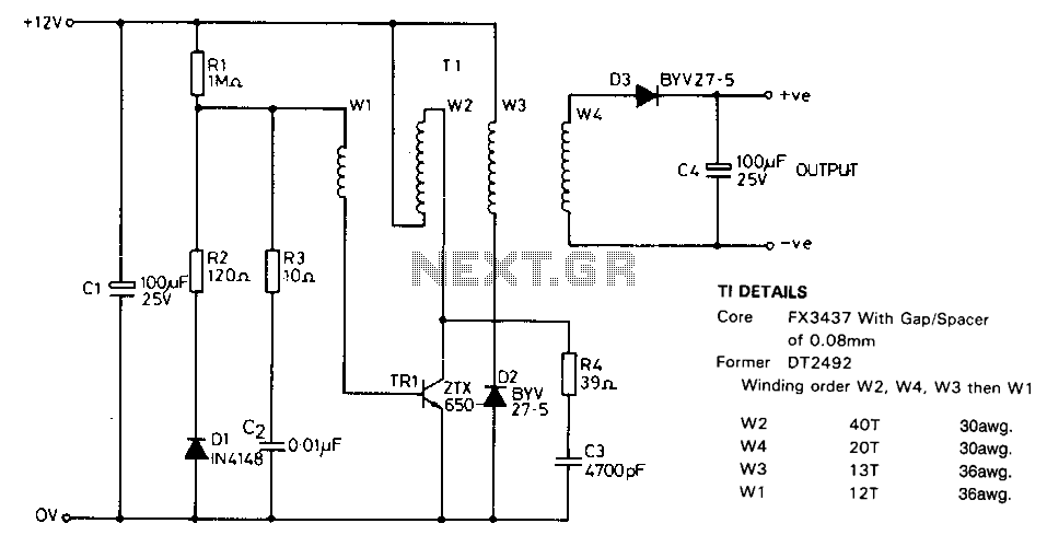
This circuit is designed to charge NiCad battery packs within the voltage range of 4.8 to 15.6 V using a convenient remote power source, such as an automobile battery. Upon initial power application, a small bias current supplied by resistor R1 through winding W1 begins to activate transistor TR1. This action generates a voltage across winding W2, and the positive feedback from the coupling between W1 and W2 fully turns on the transistor, applying the entire supply voltage across W2. The base drive voltage induced across W1 causes the junction between R1 and R2 to become negative relative to the 0-V supply, which forward-biases diode D1, providing the necessary base current to keep TR1 activated. As the transistor remains on, a magnetizing current builds up in W2, eventually saturating the ferrite core of transformer T1. This saturation leads to a sudden increase in the collector current flowing through TR1, resulting in a rise in its collector-emitter voltage and a decrease in the voltage across W2. The current in W2 causes the collector voltage of TR1 to swing positive until limited by the load on the transformer output. The RC network consisting of resistor R4 and capacitor C3 limits the turn-off transient of TR1. Resistor R3 and capacitor C2 maintain the loop gain of the circuit when diode D1 is not conducting.
This charging circuit operates effectively by utilizing a feedback mechanism that enhances the performance of the transistor switch, TR1. The initial bias current from resistor R1 is crucial for initiating the operation, allowing the circuit to self-start. The transformer T1 plays a vital role in energy transfer, with windings W1 and W2 responsible for feedback and output, respectively. The saturation of the ferrite core is a key aspect that dictates the switching behavior of TR1, as it directly influences the collector current and the voltage dynamics across W2.
The use of diode D1 ensures that the circuit remains operational by providing a path for the base current necessary to keep TR1 in the 'on' state, especially when the input voltage fluctuates or when the load conditions change. The RC network formed by R4 and C3 is particularly important for managing the transient response of the circuit, preventing excessive voltage spikes that could damage the transistor or other components.
In addition, the combination of R3 and C2 is essential for maintaining stability in the feedback loop, ensuring that the circuit can adjust to varying conditions without losing control or oscillating undesirably. This design is particularly suitable for applications involving NiCad batteries, where controlled charging is critical to avoid overcharging and potential damage to the battery packs. Overall, this circuit exemplifies a well-engineered approach to battery charging, leveraging feedback mechanisms and component interactions to achieve efficient and reliable operation.This circuit was designed to charge NiCad battery packs in the range of 4.8 to 15.6 V from a convenient remote power source, such as an automobile battery. When power is first applied to the circuit, a small bias current supplied by Rl via winding Wl, starts to turn on the transistor TRl.
This forces a voltage across W2 and the positive feedback given by the coupling of Wl and W201uses the transistor to turn hard on, applying the full supply across W2. The base drive voltage induced across Wl makes the junction between Rl and R2 become negative with respect to the 0-V supply, forward-biasing diode Dl to provide the necessary base current to hold TRl on. With the transistor on, a magnetizing current builds up in W2, which eventually saturates the ferrite core of transformer Tl.
This results in a sudden increase on the collector current flowing through TRl, causing its collector-emitter voltage to rise, and thus reducing the voltage across W2. The current flowing in W2 forces the collector voltage of the TRl to swing positive until restricted by transformer output loading.
Rc network R4 and C3limits the turn off transient TRl. R3 and C2 maintain the loop gain of the circuit when diode Dl is not conducting. 🔗 External reference
Warning: include(partials/cookie-banner.php): Failed to open stream: Permission denied in /var/www/html/nextgr/view-circuit.php on line 713
Warning: include(): Failed opening 'partials/cookie-banner.php' for inclusion (include_path='.:/usr/share/php') in /var/www/html/nextgr/view-circuit.php on line 713