
Portable-rf-burst-generator
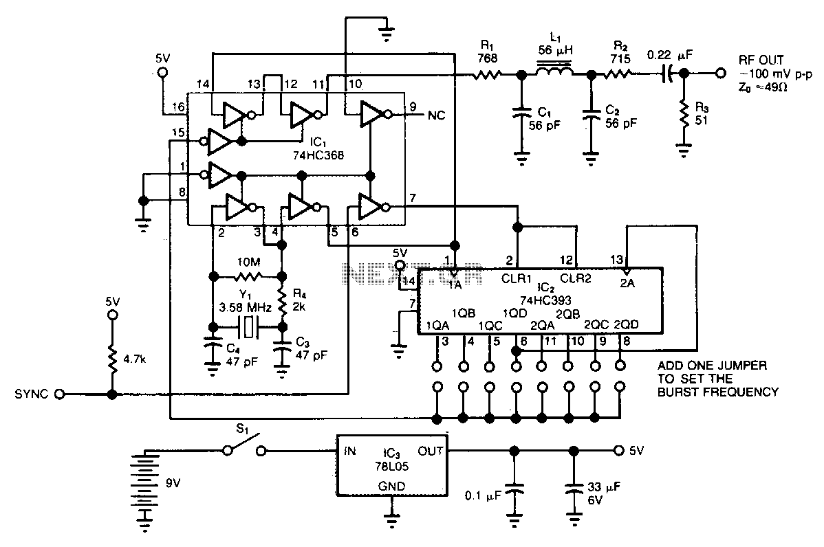
The circuit generates low-level RF bursts with frequencies up to 10 MHz, allowing for field testing of high-frequency receivers. A jumper-selectable binary fraction (1/2 to 1/256) of the Y1 crystal frequency gates the output RF signal. The output amplitude (open circuit) is approximately 100 mV, and the output impedance is around 49 ohms. The RF source consists of a clock oscillator based on a 3.58-MHz color-burst crystal and two inverting buffers. The oscillator drives two cascaded 4-bit binary counters, with the sync signal resetting the counters using a logic-high pulse followed by a logic-low state.
To select the desired output frequency, a jumper can be added to one of the counter's eight output lines, which provides an enable signal for the two 3-state output buffers. The square-wave output at pin 11 of IC1 is attenuated by resistors R1, R2, and R3 to maintain an output resistance of approximately 49 ohms. Resistor R3 is the only critical component; for optimal gating performance, it should be isolated from the rest of the circuit.
The circuit design primarily focuses on generating a stable RF signal suitable for testing high-frequency receivers. The use of a 3.58-MHz color-burst crystal ensures that the oscillator operates at a frequency that is easily divisible, allowing the circuit to produce a range of frequencies through the binary counters. The cascaded 4-bit binary counters provide a straightforward method for frequency division, enabling the selection of various output frequencies by simply changing the jumper configuration.
The output stage includes two 3-state buffers, which allow for a clean transition between different output states without impacting the overall circuit performance. The attenuation provided by resistors R1, R2, and R3 is crucial for maintaining the desired output impedance, ensuring compatibility with various testing equipment. The careful selection of R3 as a critical component highlights the importance of maintaining signal integrity during operation.
Overall, this circuit serves as an effective tool for generating RF signals for testing purposes, with its modular design allowing for flexibility in output frequency selection and ensuring reliable performance in field testing scenarios.The circuit generates low-level rf bursts having frequencies as high as 10 MHz, thus permitting field testing of high frequency receivers. A jumper-selectable binary fraction (liz to "1256 of the Y1 crystal frequency gates the output rf signal.
Output amplitude (open circuit) is approximately 100 mV; output impedance is approximately 49 0. The rf source is a clock oscillator based on a 3.58-MHz, color-burst crystal and two inverting buffers. The oscillator drives two cascaded 4-bit binary counters, IC2, and the sync signal resets the counters with a logic-high pulse-logic low at the counters.
Select the desired output frequency by adding a jumper to one of the counter"s eight output lines, which provides an enable signaHor the two 3-state output buffers. The square-wave output at IC1, pin 11, is attenuated by R1, R2, and R3 to fix the output resistance at approximately 49 0.
Resistor R3 is the only critical component; for clean gating, isolate it from the rest of the circuit. 🔗 External reference