
Power cipher scheme on the basis of TMS320C6678 DSP
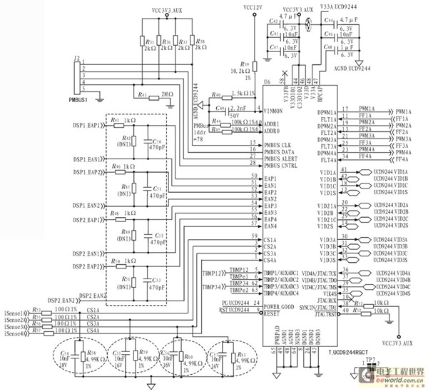
The TMS320C6678 DSP, as part of the KeyStone architecture, is designed for high-performance signal processing applications. It is equipped with eight processing cores, allowing for parallel processing capabilities that enhance throughput and efficiency in demanding applications. The architecture's ability to reach operating speeds of up to 10 GHz makes it suitable for real-time processing tasks in various fields, including telecommunications, industrial automation, and multimedia processing.
In this power management design, the UCD9244 plays a pivotal role, providing advanced control over the power supply. It employs a digital interface that allows for precise voltage regulation and monitoring, which is essential for maintaining the operational integrity of the DSP. The integration of the UCD7242 components ensures that the core voltage levels are maintained within specified limits, which is critical for the reliable performance of the DSP under varying load conditions.
The TPS54620 is included in the design to supply auxiliary power, ensuring that all components receive stable voltage levels necessary for their operation. The design incorporates extensive filtering techniques, such as LC filters, to minimize electromagnetic interference (EMI) and ensure a clean power supply to the DSP. This is particularly important in high-frequency applications where noise can significantly impact performance.
The power-up sequence is meticulously planned to ensure that the DSP and its associated components are powered in a controlled manner, which is vital for preventing damage during startup. The inclusion of an LED indicator serves a dual purpose: it not only provides a visual confirmation of the power status but also aids in troubleshooting by indicating potential faults in the system.
Overall, this power management design for the TMS320C6678 DSP exemplifies a comprehensive approach to ensuring reliable operation in high-performance applications, addressing both the stringent power requirements of the DSP and the need for robust protection and monitoring features.TMS320C6678 DSP is a section of DSP based on KeyStone framework that TI released newly, have 8 kernel, the intersection of operating speed and until the the intersection of product and of various fields performance index increase reachable 10 GHz. while being on-chip, having proposed very high requirement too for the power supply, the ordinary sta
bilized voltage supply can`t be satisfied. Because mostly need lamellar DSP collaborative work on the present SIGPROC signal processing boards, so in this design, take bivalve 6678DSP power scheme as examples, regard UCD9244 as the main control chip of the power, power supply demand that the power designed can meet this bivalve DSP at the same time. Fig. 1 is a systematic composition block diagram. Adopt the unitary 12 V power to supply power, the kernel voltage of DSP is made up of a slice of UCD9244 and bivalve UCD7242; 3.
3 V power produced through TPS54620 can be the electrical supply of the miscellaneous power; The big partial module power needs treatment filtered the wave network, can reduce the ripples, noises of the power to do it in this way, can well solve other interference problems that PCB fabric board brings at the same time. Though DSP does not require that there is sequence of special power up between kernel voltage and IO, when the power with a certain module is in error condition, must guarantee all power of the overall system is not working, otherwise, will influence life time and reliability of the device seriously.
So, in this design, the sequence of power up is CVDD, VCC1V0, VCC1V8, VCC1V5, VCC0V75; CVDD and the intersection of power up and sequence of VCC1V0, through carry on the intersection of programming and realization to the intersection of UCD9244 and chip, other the intersection of power up and sequence of module pass the TPS3808 series chip among them, the previous first grade produced the control signal to realize back first grade. Sequence and power up sequence of power down are totally opposite, so can prevent the occurrence of a large number of quiescent current and device overvoltage situation.
Any DC/DC converter, while beginning to design, the choice of operating frequency is very key. It mainly depends on 3 factors: Maximum efficiency, minimum dimension and closed loop bandwidth. Operating frequency is high, usually efficiency is low, the design size is small. Consider synthetically, in this design, choose 750 kHz. At the end that is designed, supplying power for the key power adds the pilot lamp of signals partly, if power up can make LED to be bright while being normal, it to debug for convenience mainly in role in circuit, meanwhile, can find at once which module makes mistakes when the power up of the circuit is abnormal, thus can find the reason quickly. UCD9244 chip is a figure PWM control device, can control No. 4 to export at the same time, switching frequency reaches 2 MHz, adopt PMBus v1. 2 standard. PMBus is a bus line of power management, came over from SMBus development, exchange with the power converter on the digital communication bus.
Fig. 2 is controlling the circuit diagram of UCD9244, the regulation of the output voltage mainly has two ways, one kind is through VID interface, this way needs the control of DSP or application-specific integrated circuit, but actually in this design was as the power of DSP, so adopted another accommodation mode Through PMBus command statement, controls the amplitude of output voltage, this way is simpler and effectiver too. In order to guarantee UCD9244 works wholly, has increased the bypass capacitor in the input end of working voltage to reduce the voltage ripple, increased the protection measure to abnormal circumstances such as high temperature, excessive load, etc.
at the same time. The intersection of Fig. and 2 UCD9244 control circuit diagram TMS320C6678 DSP one based on KeyStone framework DSP that TI release newly, have 8 kern 🔗 External reference
Related Circuits
It is important to note that there is limited protection circuitry and fuses in this amplifier. A short turn-on delay for the output power supply is included to minimize thumps, along with a couple of line fuses, but no...
Micropower and low-voltage operational amplifiers enable the construction of high-performance analog signal processors that do not require batteries or wall transformers. Instead, a capacitor can serve as the power source. The circuit illustrated in Figure 1 depicts an analog...
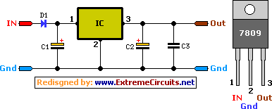
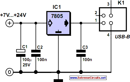
This circuit primarily relies on a voltage regulator. The 7809 voltage regulator can provide a continuous output of up to 2 amps while ensuring a low noise and highly regulated supply. Although the circuit can function without additional components,...
An increasing number of devices are being sold that operate on internal rechargeable batteries. While a compatible charger is typically included in the packaging, there are a... Rechargeable battery systems have become prevalent in various electronic devices, necessitating the development...
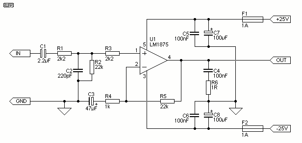
This project is based almost directly on the typical application circuit in the National Semiconductor specification sheet. You can also use the TDA2050 (from SGS-Thompson), which has almost identical performance and (remarkably) the same pinouts! As it turns out,...
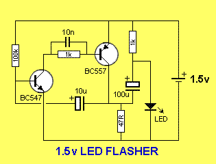
This is a simple 1.5V powered LED flasher circuit diagram. This circuit can flash 1.7V or 2.3V LEDs (depending on the color) using a 1.5V DC input. The LED will turn on when the 100µF capacitor is charged by...
Warning: include(partials/cookie-banner.php): Failed to open stream: Permission denied in /var/www/html/nextgr/view-circuit.php on line 713
Warning: include(): Failed opening 'partials/cookie-banner.php' for inclusion (include_path='.:/usr/share/php') in /var/www/html/nextgr/view-circuit.php on line 713