
Programmable-amplifier
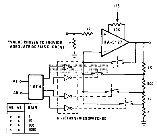
A circuit may often be required to perform multiple functions. In these cases, the variable gain configuration of the circuit can be particularly advantageous. This programmable gain stage utilizes CMOS analog switches to modify the feedback amount, thereby adjusting the stage's gain. The positioning of the switching elements within the relatively low-current region of the feedback loop minimizes the impact of bias currents and switch resistance on the calculated gain of the stage. Voltage spikes can occur during the switching process, leading to a temporary reduction in gain due to the make-before-break operation of the switches. This gain reduction can be mitigated by implementing a separate voltage divider network for each gain level.
The described circuit operates as a programmable gain amplifier (PGA), which is essential in applications requiring adaptable signal amplification. The use of CMOS analog switches allows for precise control over the feedback network, enabling the gain to be dynamically adjusted based on the input signal or system requirements.
In this configuration, the feedback loop is crucial for maintaining stability and linearity of the gain. By placing the analog switches in a low-current section of the feedback loop, the circuit effectively reduces interference from bias currents, which can otherwise skew the gain calculations. This design choice enhances the performance of the amplifier in precision applications, such as instrumentation or audio processing.
The make-before-break switching mechanism is a key feature that facilitates seamless transitions between different gain settings. However, it can introduce voltage spikes, which may temporarily affect the gain. To counteract this issue, each gain setting is supported by a dedicated voltage divider network. This network helps to stabilize the output voltage during transitions and ensures that the gain remains consistent across different operating conditions.
By employing this sophisticated approach, the circuit achieves a high degree of versatility and reliability, making it suitable for a wide range of electronic applications where adjustable gain is necessary.Often a circuit will be called upon to perform several functions. In these situations, the variable gain configuration of this circuit could be quite useful. This programmable gain stage depends on CMOS analog switches to alter the amount of feedback, and thereby, the gain of the stage. Placement of the switching elements inside the relatively lowcurrent area of the feedback loop, minimizes the effects of bias currents and switch resistance on the calculated gain of the stage.
Voltage spikes can occur during the switching process, resulting in temporarily reduced gain because of the makebefore- break operation of the switches. This gain loss can be minimized by providing a separate voltage divider network for each level of gain.
🔗 External reference