
PULSE DELAY
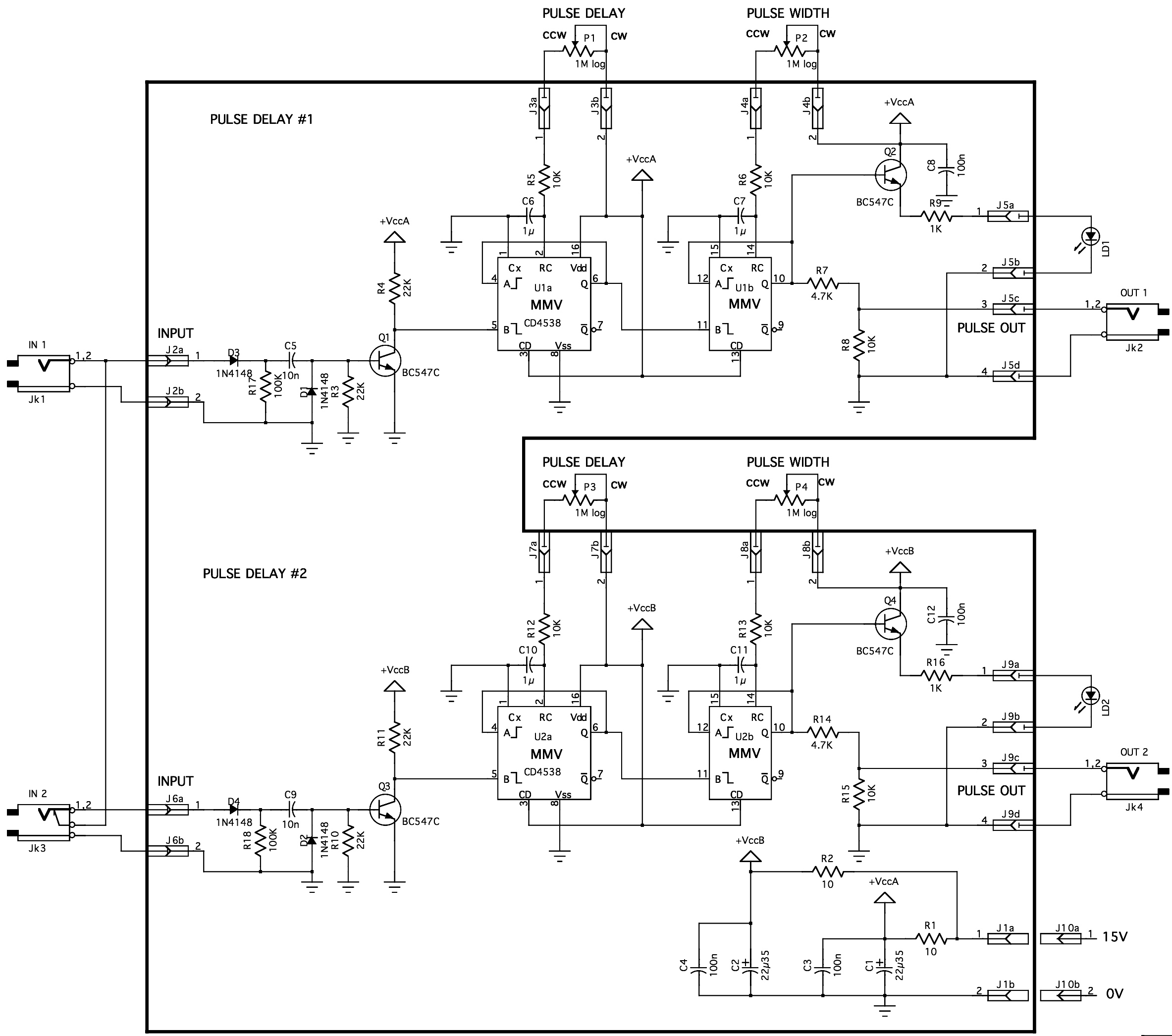
The described circuit operates in response to a GATE signal within a specified voltage range. The initial differentiating action of capacitor C5 is crucial for generating a precise pulse, which is then used to control subsequent monostable multivibrators (U1a and U1b). The first monostable multivibrator (U1a) is configured to output a high signal for a period defined by the time constant of the RC combination of resistor R5, potentiometer P1, and capacitor C6. The choice of a logarithmic potentiometer allows for finer control over the timing, making it suitable for applications requiring variable pulse widths.
Upon receiving the pulse, Q1 momentarily conducts, pulling the collector voltage low, which is essential for triggering U1a. The output from U1a then initiates a second timing sequence through U1b, utilizing a similar RC timing configuration with R6, P2, and C7. This second stage is designed to ensure that the output pulse duration can also be finely adjusted, providing versatility in the circuit's operation.
The voltage divider formed by resistors R7 and R8 is instrumental in scaling the output pulse to 10V, making it suitable for interfacing with other components or systems that require a specific voltage level. The final output drives an LED (LD1) through transistor Q2, providing a visual indication of the output pulse. The use of transistors for driving the LED ensures that the circuit can handle the necessary current without compromising the integrity of the timing circuit. Overall, this configuration allows for precise control of pulse generation, making it useful in a variety of electronic applications, such as signal processing, timing applications, and control systems.When a GATE signal (between 3V and 15V), the capacitor C5 acts as a differenciator and converts the gate signal into a brief positive pulse (width 10 ms). D1 protects the circuit from negative voltages. The brief pulse created on the rising edge of the GATE signal make Q1 briefly conductive and the voltage at its collecto
r falls down to 0. 2V. The collector is connected to the falling edge trigger pin of U1a. This triggers the monostable U1a and its output Q goes to a high level and stays there for a duration set by the RC cell built around (R5+P1)C6, P1 is a 1M log potentiometer and the delay can be set between 1ms and 1s. After this delay Q returns to the low level and in turn triggers the second monostable U1b whose output Q goes to the high level and stays there for a duration set by the RC cell built around (R6+P2)C7, P2 is a 1M log potentiometer and the delay can be set between 1ms and 1s.
The output Q is connected to a voltage divider (R7, R8) that delivers the OUTPUT PULSE with a amplitude of 10V. The base of Q2 is connected to the Q output of U1b and drives the LD1 LED. 🔗 External reference
Related Circuits
This circuit is a robust light control delay switch with strong anti-interference capabilities. It requires a specific sequence of claps to activate the lamp, which will illuminate for a predetermined duration before automatically turning off. The circuit design is...
The TN-1 Intelligent Negative Pulse Charging Circuit is a sophisticated device designed for efficient battery charging. It operates as a half-bridge charger, which is a common configuration in such circuits. The negative pulse charging mechanism is facilitated by a...
This circuit is designed to provide long time delays using the integrated circuit Timer 555. It utilizes the NE555 to generate pulse frequencies, which are then divided by a 4017 decade counter to achieve the desired delay. The component...
The circuit described here was designed as an addition to a remotely controlled garage door opener. The problem was that a brief burst of interference, arising from a thunderstorm or a mains spike, was enough to trigger the mechanism,...
The D-type flip-flop IC2 is designed to synchronize the input signal with the clock pulse. When the clock pulse transitions from low to high and the input is high, the output of IC2 becomes high. This condition subsequently resets...

An NE555 timer integrated circuit (IC) configured in a specific manner can identify the absence of a pulse or an unusually long duration between two successive pulses in a pulse train. Such circuits are applicable for detecting the intermittent...
Warning: include(partials/cookie-banner.php): Failed to open stream: Permission denied in /var/www/html/nextgr/view-circuit.php on line 713
Warning: include(): Failed opening 'partials/cookie-banner.php' for inclusion (include_path='.:/usr/share/php') in /var/www/html/nextgr/view-circuit.php on line 713