Pulse Width Modulation
1. Definition and Basic Principles
1.1 Definition and Basic Principles
Pulse Width Modulation (PWM) is a technique for encoding analog signal levels into a digital signal by varying the duty cycle of a periodic square wave. The fundamental principle relies on controlling the average power delivered to a load by rapidly switching between fully on and fully off states. Mathematically, the average voltage Vavg of a PWM signal is given by:
where D is the duty cycle (0 ≤ D ≤ 1) and Vpeak is the amplitude of the pulse. The duty cycle represents the fraction of time the signal is in the high state relative to the total period T:
Time-Domain Characteristics
A PWM signal is fully characterized by three parameters:
- Frequency (f): The inverse of the period T, determining how often the pulse repeats.
- Amplitude (Vpeak): The voltage level during the ton phase.
- Duty Cycle (D): The ratio of pulse width to period, directly controlling the average output.
Fourier Analysis of PWM
In the frequency domain, a PWM signal contains harmonic components at integer multiples of the fundamental frequency. The spectral composition can be derived from the Fourier series expansion of a periodic pulse train:
This reveals that harmonic amplitudes follow a sinc envelope, with nulls occurring at frequencies fnull = k/(DT) for integer k.
Practical Implementation Considerations
Real-world PWM systems must account for:
- Switching losses: Non-ideal transitions in power electronics cause energy dissipation proportional to frequency.
- Dead time: Intentional delays between complementary switches to prevent shoot-through currents.
- Load impedance: Inductive loads require freewheeling diodes to handle current continuity during off periods.
Applications in Power Electronics
PWM serves as the foundation for:
- Switch-mode power supplies (buck/boost converters)
- Motor speed control in H-bridge configurations
- Class-D audio amplification
- LED dimming through current averaging
1.2 Duty Cycle and Frequency
Definition of Duty Cycle
The duty cycle (D) of a pulse width modulated (PWM) signal is defined as the ratio of the pulse duration (ton) to the total period (T) of the waveform. Mathematically, this is expressed as:
For a square wave with equal on and off times, the duty cycle is 50%. In power electronics applications, duty cycles typically range from 0% (fully off) to 100% (fully on), with precise control enabling efficient energy delivery.
Relationship Between Duty Cycle and Average Voltage
The time-averaged voltage (Vavg) of a PWM signal with amplitude Vmax is directly proportional to its duty cycle:
This linear relationship forms the basis for PWM-based digital-to-analog conversion and motor speed control. For instance, a 12V PWM signal with 25% duty cycle delivers an effective 3V average voltage to a load.
Frequency Considerations
The PWM frequency (f) is the reciprocal of the period:
Selection of appropriate frequency involves tradeoffs between:
- Switching losses: Higher frequencies increase MOSFET/IGBT switching losses
- Filtering requirements: Lower frequencies require larger LC filters
- Load characteristics: Motors typically use 5-20kHz, while LEDs may use 100Hz-1kHz
Harmonic Content Analysis
The Fourier series expansion of a PWM signal reveals its harmonic spectrum. For a duty cycle D and fundamental frequency f0, the normalized amplitude of the nth harmonic is:
This shows harmonic nulls at duty cycles where nD is integer-valued. Modern PWM controllers use spread-spectrum techniques to mitigate electromagnetic interference (EMI) from these harmonics.
Practical Implementation Constraints
Real-world PWM systems face several implementation limits:
- Minimum pulse width: Dictated by semiconductor switching speeds (typically 50-500ns)
- Dead time: Required to prevent shoot-through in H-bridge configurations
- Resolution limits: Digital controllers have finite duty cycle granularity (8-16 bits typical)
Modern microcontrollers implement advanced PWM features like:
- Edge-aligned vs center-aligned modulation
- Complementary output with programmable dead time
- Burst mode operation for ultra-low power applications
Thermal Implications
The power dissipation in switching elements follows:
where Eon and Eoff are the switching energy losses. This equation highlights the frequency-dependent nature of switching losses, which become dominant above 100kHz for silicon MOSFETs.
1.3 Analog vs. Digital PWM Signals
Fundamental Differences in Signal Generation
Pulse Width Modulation (PWM) can be implemented using either analog or digital techniques, each with distinct characteristics. Analog PWM generation relies on continuous-time comparison between a modulating signal (typically a sine or triangle wave) and a reference signal. The output duty cycle varies smoothly as:
where Vmod(t) is the time-varying analog input and Vref is the peak reference voltage. In contrast, digital PWM employs discrete-time counters and comparators, quantizing the duty cycle into 2N steps where N is the bit resolution:
Spectral Characteristics and Noise Performance
Analog PWM exhibits a continuous spectrum with harmonic energy concentrated at integer multiples of the switching frequency fsw. The baseband noise floor follows a 1/f characteristic due to analog component imperfections. Digital PWM introduces quantization noise:
where Δ is the duty cycle step size (1/2N) and fs is the update rate. Modern hybrid approaches use sigma-delta modulation to shape quantization noise away from the signal band.
Implementation Tradeoffs
- Analog Advantages: Infinite resolution, lower electromagnetic interference (EMI) at high frequencies due to smoother transitions
- Digital Advantages: Precision immune to component drift, programmable frequency/phase, easier synchronization in multi-channel systems
- Hybrid Techniques: Combining analog integrators with digital control loops achieves sub-LSB resolution while maintaining stability
Application-Specific Considerations
In motor control, analog PWM reduces torque ripple but requires careful temperature compensation. Digital PWM dominates in switched-mode power supplies where >10-bit resolution enables precise voltage regulation. RF applications often use digital implementations for phase-coherent control of GaN transistors, leveraging the precise timing of FPGA-based generators.
2. Hardware-Based PWM Generation
2.1 Hardware-Based PWM Generation
Timer-Counter Modules in Microcontrollers
Most microcontrollers implement hardware-based PWM generation using dedicated timer-counter modules. These modules consist of a counter register that increments or decrements at a fixed clock rate, along with one or more compare registers that define the duty cycle. When the counter matches a compare register value, the output pin toggles, generating a PWM signal. The frequency is determined by:
where fCLK is the timer clock frequency, N is the prescaler value, and TOP is the maximum counter value (e.g., 255 for an 8-bit timer). The duty cycle D is set by the compare register CCR:
Dedicated PWM Controller ICs
For high-precision applications, dedicated PWM controller ICs such as the TL494 or SG3525 provide advanced features including:
- Dead-time control to prevent shoot-through in H-bridge configurations
- Synchronization inputs for multi-phase operation
- Error amplifiers for closed-loop feedback
These devices typically use a sawtooth or triangle waveform generator compared against a reference voltage to produce PWM outputs. The oscillation frequency is set by an external RC network:
FPGA-Based Implementation
In FPGAs, PWM generation is achieved through digital logic using:
- A free-running counter for the carrier waveform
- Comparators for duty cycle control
- Optional dithering logic for improved resolution
The minimal clock cycles required per PWM period in an FPGA implementation is given by:
where n is the bit resolution of the PWM signal. Modern FPGAs can achieve PWM frequencies exceeding 100 MHz with sub-nanosecond edge placement accuracy.
Analog PWM Generation
Before digital methods became prevalent, analog techniques were used, such as:
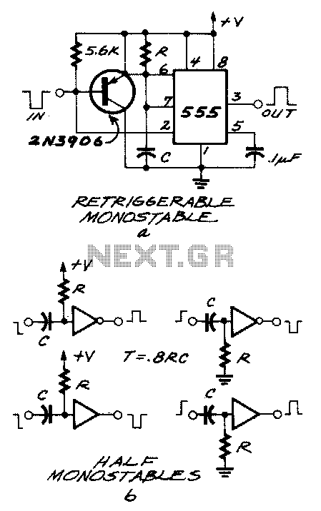
- Triangle-wave comparison: An op-amp integrator generates a triangle wave which is compared against a DC control voltage
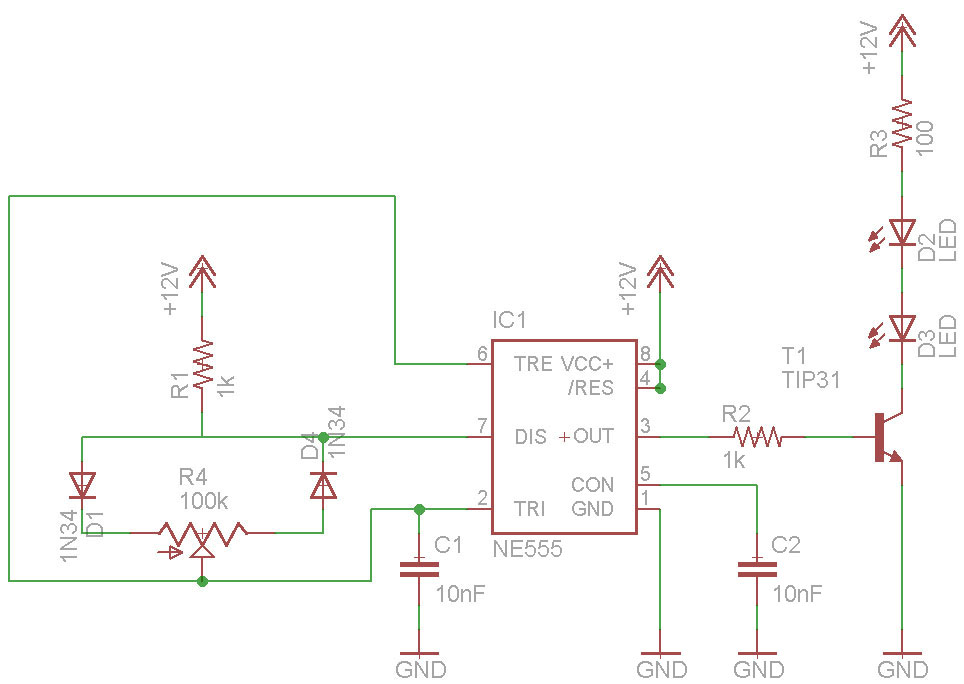
- 555 timer circuits: Using the 555 in astable mode with modulation input on the control pin
The analog approach remains useful for ultra-high frequency applications (>1 MHz) where digital propagation delays become significant. The duty cycle in an analog comparator-based system is linearly proportional to the control voltage:
Power Stage Considerations
Hardware PWM implementations must account for power stage requirements:
- Gate drive current: MOSFET switching losses scale with PWM frequency
- Dead time: Necessary to prevent cross-conduction in half-bridge topologies
- EMI suppression: Higher dv/dt at increased frequencies requires careful layout
The power dissipation in switching devices can be estimated by:
where tr and tf are the rise and fall times of the power device.
2.2 Software-Based PWM Generation
Software-based PWM generation leverages programmable timers and interrupts in microcontrollers to produce precise pulse-width modulated signals without dedicated hardware peripherals. This approach is particularly useful in resource-constrained embedded systems where hardware PWM modules are unavailable or already occupied.
Timer-Based PWM Implementation
Most microcontrollers feature general-purpose timers that can be configured to generate PWM signals. The process involves:
- Configuring the timer in PWM mode or output compare mode.
- Setting the timer's period register to determine the PWM frequency.
- Adjusting the duty cycle register to control the pulse width.
The PWM frequency (fPWM) is determined by the timer's clock source and period register value:
where ftimer is the timer clock frequency and PR is the value loaded into the period register.
Interrupt-Driven PWM
When hardware PWM is unavailable, an interrupt-driven approach can emulate PWM behavior:
- Configure a timer to trigger an interrupt at the desired PWM frequency.
- In the interrupt service routine (ISR):
- Set the output pin high at the start of each period.
- Use a second timer or counter to determine when to clear the pin based on the duty cycle.
This method introduces jitter due to interrupt latency but remains effective for low-frequency applications (typically below 1 kHz).
PWM Resolution and Tradeoffs
The number of discrete duty cycle steps (resolution) is given by:
Higher resolution requires larger period register values, which reduces the maximum achievable PWM frequency. The relationship between frequency and resolution is:
where n is the desired resolution in bits.
Advanced Techniques
Modern implementations often employ:
- Double buffering to update PWM parameters synchronously
- Dead-time insertion for motor control applications
- Dithering to achieve effective resolution beyond hardware limits
For example, a 16-bit microcontroller running at 48 MHz can theoretically generate:
at 16-bit resolution, or 187.5 kHz at 8-bit resolution.
Real-World Considerations
Practical implementations must account for:
- Interrupt latency effects on timing precision
- CPU loading from ISR overhead
- Timer peripheral limitations in low-power devices
- Electromagnetic interference from software-generated signals
In motor control systems, software PWM often incorporates closed-loop feedback to compensate for these limitations, using techniques like adaptive dead-time adjustment and dynamic frequency scaling.
2.3 Microcontroller PWM Modules
Modern microcontrollers integrate dedicated hardware peripherals for generating Pulse Width Modulation (PWM) signals with high precision and minimal CPU overhead. These modules operate by comparing a timer counter against a programmable duty cycle register, generating a digital output that toggles when a match occurs. The fundamental components include:
- Timer/Counter: A free-running or up/down counter clocked by the system clock or a prescaled derivative.
- Compare Registers: Store the duty cycle value (e.g.,
CCRxin ARM or AVR architectures). - Output Control Logic: Manages polarity, dead-time insertion, and synchronization.
Mathematical Foundation
The PWM frequency (fPWM) is determined by the timer's clock source (fCLK) and the period register (ARR for Auto-Reload Register in STM32, or TOP in AVR):
where PRESCALER divides the input clock, and ARR sets the maximum timer value. The duty cycle (D) is calculated as:
Advanced Features
High-end microcontrollers (e.g., STM32, PIC32, ESP32) support:
- Complementary Outputs: Paired PWM signals with programmable dead-time for H-bridge control.
- Burst Mode: DMA-driven updates to duty cycles without CPU intervention.
- Center-Aligned PWM: Counters that increment and decrement to reduce EMI in motor drives.
Register-Level Configuration Example
For an STM32F4 using Timer 1 (general-purpose timer) in PWM mode:
// Configure Timer 1 Channel 1 for PWM @ 20 kHz
TIM1->PSC = 83;                          // Prescaler = 84-1 (1 MHz clock from 84 MHz)
TIM1->ARR = 49;                          // Auto-reload = 50-1 (20 kHz PWM)
TIM1->CCR1 = 25;                         // 50% duty cycle
TIM1->CCMR1 |= TIM_CCMR1_OC1M_2 | TIM_CCMR1_OC1M_1;  // PWM mode 1
TIM1->CCER |= TIM_CCER_CC1E;             // Enable output
TIM1->CR1 |= TIM_CR1_CEN;                // Start timer
Practical Considerations
Edge cases require attention:
- Resolution Tradeoffs: Higher PWM frequencies reduce duty cycle granularity. For a 16-bit timer at 100 kHz (fCLK = 80 MHz), maximum resolution is 12 bits (80 MHz / 100 kHz = 800 counts).
- Glitch Prevention: Shadow registers (e.g., STM32's preload feature) ensure atomic updates to period/duty values.
- EMI Mitigation: Spread-spectrum PWM randomization techniques in microcontrollers like dsPIC33 reduce peak emissions.
Real-world applications leverage these features in motor control (field-oriented control), power converters (buck/boost topologies), and digital audio (class-D amplifiers).
3. Motor Speed Control
3.1 Motor Speed Control
Fundamentals of PWM-Based Speed Regulation
The average voltage delivered to a DC motor is governed by the duty cycle (D) of the PWM signal, defined as the ratio of the pulse width (Ï„) to the signal period (T). The effective voltage (Veff) is derived as:
For brushless DC (BLDC) or stepper motors, PWM modulates current through the stator windings, with torque proportional to the RMS current. The relationship between duty cycle and angular velocity (ω) in a DC motor with back-EMF constant (ke) and armature resistance (Ra) is:
Switching Frequency Considerations
The PWM frequency (fPWM) must exceed the motor's mechanical time constant to avoid audible noise and torque ripple. For a motor with inductance L and time constant Ï„m = L/Ra, the minimum frequency is:
Typical industrial applications use 5–20 kHz, balancing switching losses (MOSFET/IGBT) and current ripple. High-frequency PWM (>50 kHz) reduces acoustic noise but increases gate driver losses.
Dead-Time Insertion
In H-bridge configurations, dead-time (td) prevents shoot-through currents during transistor switching. The minimum dead-time is determined by the driver propagation delay (tpd) and transistor turn-off time (toff):
Dead-time introduces nonlinearity in motor voltage, compensated via feedforward algorithms or adaptive timing control.
Closed-Loop Speed Control
PID controllers adjust the PWM duty cycle based on encoder feedback. The error (e(t)) between desired (ωref) and measured speed (ωm) generates the control signal:
Implementation note: Anti-windup techniques are critical to prevent integrator saturation during motor stalling.
Practical Design Example
For a 24V, 200W DC motor (Ra = 0.5Ω, L = 2mH, ke = 0.05 V/rpm):
- PWM frequency: 10 kHz (τm = 4 ms → 40× margin)
- Dead-time: 500 ns (IR2110 driver + SiC MOSFET)
- PID gains: Kp=0.8, Ki=12, Kd=0.001 via Ziegler-Nichols tuning
3.2 LED Brightness Control
Pulse Width Modulation (PWM) is a highly efficient method for controlling LED brightness by rapidly switching the power supply on and off. The perceived brightness is determined by the duty cycle—the ratio of the on-time to the total period of the signal. For an LED driven by a PWM signal with a frequency sufficiently high to avoid visible flicker (typically above 60 Hz), the average current through the LED is given by:
where D is the duty cycle (0 ≤ D ≤ 1) and Ipeak is the peak current when the LED is fully on. The human eye integrates light over time, perceiving the LED as dimmer when the duty cycle decreases.
Mathematical Derivation of Brightness Control
The relationship between duty cycle and luminous flux can be derived from the LED's forward current (IF) versus luminous intensity (Φv) characteristics. Assuming a linear approximation:
where K is the luminous efficacy (in lumens per ampere). Combining this with the PWM-driven average current:
Thus, the perceived brightness scales linearly with the duty cycle. However, at very low duty cycles (D < 5%), nonlinearities may arise due to the LED's threshold voltage and transient response.
Practical Implementation Considerations
For precise brightness control, the following factors must be considered:
- PWM Frequency: Must be high enough to avoid flicker (≥100 Hz for most applications). However, excessively high frequencies can introduce switching losses in the driving circuit.
- LED Forward Voltage: The PWM signal must ensure the LED operates within its specified forward voltage range during the on-state.
- Current Limiting: A series resistor or constant-current driver is necessary to prevent excessive Ipeak during the on-time.
Microcontroller-Based PWM Generation
Modern microcontrollers (e.g., ARM Cortex-M, AVR, PIC) include hardware PWM peripherals that allow precise duty cycle control. For example, an 8-bit PWM resolution provides 256 discrete brightness levels. The duty cycle register value (OCR) is set as:
where n is the PWM resolution in bits. Higher resolutions (e.g., 12- or 16-bit) enable smoother dimming but require faster PWM clocks or longer periods.
Visual Representation of PWM Brightness Control
A diagram illustrating PWM-driven LED brightness would show:
- A square wave with varying duty cycles (e.g., 10%, 50%, 90%).
- The corresponding LED intensity, demonstrating how higher duty cycles result in brighter output.
- The average current waveform superimposed on the PWM signal.
Advanced Techniques: Gamma Correction
Human vision perceives brightness logarithmically, not linearly. To achieve perceptually uniform brightness steps, gamma correction is applied by mapping the desired brightness level L (0 to 1) to a corrected duty cycle D:
where γ ≈ 2.2 for typical LEDs. This ensures equal steps in perceived brightness when adjusting the PWM duty cycle.
Applications in High-Power LED Systems
PWM dimming is critical in high-power LED applications (e.g., automotive lighting, architectural illumination) due to its efficiency and precision. Constant-current drivers with PWM inputs (e.g., using buck/boost converters) enable scalable control without color shift, which can occur with analog dimming methods.
3.3 Power Conversion and Regulation
Pulse Width Modulation (PWM) is a cornerstone technique in power electronics, enabling precise control over power conversion and regulation. By modulating the duty cycle of a square wave, PWM allows efficient conversion of electrical power between different voltage and current levels while minimizing energy loss.
Average Voltage and Power Transfer
The average output voltage of a PWM signal is directly proportional to its duty cycle. For a PWM waveform with amplitude VDC and duty cycle D, the average voltage Vavg is:
In power regulation applications, this principle allows a DC-DC converter to step up or step down voltage by adjusting D. For instance, a buck converter reduces voltage when D < 1, while a boost converter increases it when D approaches 1. The power transferred to the load is:
where R is the load resistance. This relationship highlights how PWM enables dynamic power control without dissipative losses inherent in linear regulators.
Switching Losses and Efficiency
While PWM minimizes conduction losses, switching losses arise due to finite transition times in semiconductor devices. The total power loss Ploss in a MOSFET-based PWM converter includes:
where Psw is the switching loss and Pcond is the conduction loss. Switching loss per cycle is given by:
Here, tr and tf are the rise and fall times, and fsw is the switching frequency. High-frequency PWM reduces output ripple but increases switching losses, necessitating a trade-off in design.
Regulation via Feedback Control
Closed-loop PWM regulation employs feedback to maintain stable output despite load variations. A proportional-integral (PI) controller adjusts the duty cycle dynamically:
where e(t) is the error between desired and actual output, and Kp, Ki are tuning gains. This method is ubiquitous in switch-mode power supplies (SMPS), where it ensures tight voltage regulation under transient loads.
Real-World Applications
- Motor Drives: PWM controls torque and speed in BLDC motors by varying effective voltage.
- Renewable Energy: Solar inverters use PWM to convert DC to grid-compatible AC.
- LED Dimming: PWM adjusts brightness without color shift by modulating current pulses.
Modern implementations leverage digital signal processors (DSPs) or field-programmable gate arrays (FPGAs) to achieve nanosecond-precision PWM generation, enabling efficiencies exceeding 95% in high-power applications.
4. Dead Time in PWM Signals
4.1 Dead Time in PWM Signals
In high-power switching applications, such as motor drives and inverters, dead time is a critical parameter that prevents shoot-through currents in half-bridge or full-bridge configurations. Shoot-through occurs when both the high-side and low-side switches in a bridge are momentarily turned on simultaneously, creating a low-impedance path between the power supply and ground. This results in excessive current spikes, increased switching losses, and potential device failure.
Mathematical Derivation of Dead Time
The required dead time (tdead) depends on the turn-off delay (toff) and turn-on delay (ton) of the power switches (e.g., MOSFETs or IGBTs). For a conservative estimate, dead time must exceed the worst-case delay mismatch between the switches:
where tmargin is an additional safety margin (typically 10–100 ns) to account for gate driver propagation delays and temperature variations. If the dead time is too short, shoot-through occurs; if too long, it introduces distortion and reduces output voltage accuracy.
Impact on PWM Performance
Dead time introduces non-linearities in the output voltage waveform, particularly at low duty cycles. The effective duty cycle (Deff) deviates from the commanded duty cycle (D) due to the dead-time-induced voltage drop:
where Tsw is the switching period, and sgn(I) denotes the direction of the load current. This distortion becomes significant in high-frequency PWM systems (e.g., >20 kHz) or when driving inductive loads.
Practical Implementation Techniques
Modern gate drivers and microcontrollers integrate programmable dead-time generators to automate this process. Key implementation considerations include:
- Adaptive Dead Time: Dynamically adjusts tdead based on real-time current sensing to minimize distortion.
- Blanketing: Overlapping drive signals are suppressed using hardware interlocks in gate driver ICs (e.g., DESAT protection in IGBT drivers).
- Compensation Algorithms: Feedforward or feedback correction in digital PWM controllers to counteract dead-time effects.
Case Study: Dead Time in H-Bridge Motor Drives
In a 3-phase inverter, dead time causes voltage loss and torque ripple. Measurements on a 48V, 10A motor drive show a 5% reduction in output voltage at 10 kHz PWM due to a 500 ns dead time. This is mitigated by:
- Using fast-switching SiC MOSFETs (toff = 50 ns) to reduce dead-time requirements.
- Implementing sensorless current reconstruction to estimate and compensate for dead-time distortion.
4.2 Synchronous and Asynchronous PWM
Fundamental Differences
Synchronous PWM relies on a fixed clock signal to synchronize the switching transitions of all PWM channels, ensuring deterministic timing. In contrast, asynchronous PWM operates without a global clock, allowing independent switching frequencies for each channel. The choice between these methods depends on system requirements such as noise sensitivity, power efficiency, and computational overhead.
Synchronous PWM Operation
In synchronous PWM, a master clock dictates the PWM period, and all channels update their duty cycles at the same instant. This synchronization minimizes beat frequencies and reduces electromagnetic interference (EMI). The duty cycle D for a given channel is expressed as:
where ton is the active high time and Tclk is the clock period. Synchronous systems often employ a counter-comparator architecture, where a free-running counter resets at Tclk, and individual compare registers set the duty cycle per channel.
Asynchronous PWM Operation
Asynchronous PWM allows each channel to operate with an independent timer, enabling heterogeneous duty cycles and frequencies. This flexibility is advantageous in multi-motor control or mixed-signal systems where different loads require distinct switching rates. However, unsynchronized edges may introduce subharmonic noise and complicate filtering.
Here, Tchan is the period of the channel-specific timer. Asynchronous designs often incorporate dead-time compensation to prevent shoot-through in H-bridge configurations.
Practical Trade-offs
- Synchronous PWM excels in noise-critical applications (e.g., audio amplifiers) but requires precise clock distribution.
- Asynchronous PWM simplifies multi-rate systems (e.g., LED dimming) at the cost of increased spectral noise.
Implementation Case Study: Motor Drives
Three-phase inverters typically use synchronous PWM to maintain phase alignment, with space vector modulation (SVM) optimizing voltage utilization. Asynchronous methods appear in brushed DC motor controllers, where individual channel timing is less critical.
This effective voltage calculation highlights how synchronous PWM's fixed T simplifies RMS voltage estimation compared to asynchronous approaches.
4.3 PWM in Switching Power Supplies
Pulse Width Modulation (PWM) is a cornerstone technique in modern switching power supplies, enabling efficient voltage regulation through high-frequency switching. Unlike linear regulators, which dissipate excess power as heat, PWM-based converters modulate the duty cycle of a switching transistor to control the average output voltage with minimal losses.
Fundamental Operating Principle
In a buck converter, the output voltage Vout is determined by the input voltage Vin and the duty cycle D of the PWM signal driving the switch:
where D = t_{on} / T, ton is the ON time of the switch, and T is the switching period. The inductor and capacitor form a low-pass filter, smoothing the pulsed waveform into a stable DC output.
Control Loop Dynamics
Switching power supplies employ feedback control to maintain regulation. A voltage error amplifier compares the output with a reference, adjusting the PWM duty cycle to compensate for load or input variations. The loop gain must be carefully designed to ensure stability, often modeled using small-signal analysis:
where:
- GPWM(s) is the modulator gain (typically 1/Vramp),
- GLC(s) is the transfer function of the LC filter,
- H(s) is the feedback network gain.
Efficiency Considerations
Switching losses dominate at high frequencies due to non-ideal transistor behavior. The total power loss Ploss in a MOSFET switch includes conduction and switching components:
where tr and tf are rise/fall times, and fsw is the switching frequency. Soft-switching techniques (e.g., ZVS, ZCS) mitigate these losses by ensuring voltage or current transitions occur at zero crossings.
Advanced Topologies
Multi-phase interleaved PWM improves current handling and reduces output ripple by phase-shifting parallel converter stages. For isolated supplies, phase-shifted full-bridge topologies leverage PWM to control power transfer across transformers while minimizing circulating currents.
Synchronous rectification replaces diodes with actively controlled MOSFETs, further improving efficiency by reducing forward voltage drops. Dead-time management becomes critical to prevent shoot-through currents during switching transitions.
Practical Design Challenges
High di/dt and dv/dt rates introduce electromagnetic interference (EMI), requiring careful PCB layout and filtering. Gate drive circuits must deliver sufficient current to minimize switching times without introducing excessive noise. Modern ICs integrate adaptive dead-time control and spread-spectrum modulation to address these issues.
5. Essential Books on PWM
5.1 Essential Books on PWM
- Pulse Width Modulation For Power Converters Principles and Practice PDF — 14.1 Random Pulse Width Modulation 586 14.2 PWM Rectifier with Voltage Unbalance 590 14.3 Common Mode Elimination 598 14.4 Four Phase Leg Inverter Modulation 603 14.5 Effect of Minimum Pulse Width 607 14.6 PWM Dead-Time Compensation 612 14.7 Summary 619
- Pulse Width Modulation For Power Converters ... - E-book library — 3.4 Naturally Sampled Pulse Width Modulation. 3.5 PWM Analysis by Duty Cycle Variation. 3.6 Regular Sampled Pulse Width Modulation. 3.7 "Direct" Modulation. 3.8 Integer versus Non-Integer Frequency Ratios. 3.9 Review of PWM Variations. 3.10 Summary. Chapter 4: Modulation of Single-Phase Voltage Source Inverters. 4.1 Topology of a Single-Phase ...
- Pulse width modulation for power converters : principles and practice ... — Pulse-duration modulation; Genre(s) Electronic books; ISBN 9780470546284 electronic 9780471208143 print 047054628X electronic Bibliography Note Includes bibliographical references (pages 671-713) and index. Other Forms Also available in print. Technical Details Mode of access: World Wide Web
- Power Electronic Converters - Wiley Online Library — Power Electronic Converters PWM Strategies and Current Control Techniques Edited by ... A CIP record for this book is available from the British Library ... Introduction..... xv Chapter 1. Carrier-Based Pulse Width Modulation for Two-level Three-phase Voltage Inverters..... 1 Francis LABRIQUE and Jean-Paul LOUIS 1.1. ...
- Power Electronic Converters: PWM Strategies and Current Control ... — A voltage converter changes the voltage of an electrical power source and is usually combined with other components to create a power supply. This title is devoted to the control of static converters, which deals with pulse-width modulation (PWM) techniques, and also discusses methods for current control. Various application cases are treated. The book is ideal for professionals in power ...
- Power Electronic Converters: PWM Strategies and Current Control ... — A voltage converter changes the voltage of an electrical power source and is usually combined with other components to create a power supply. This title is devoted to the control of static converters, which deals with pulse-width modulation (PWM) techniques, and also discusses methods for current control. Various application cases are treated. The book is ideal for professionals in power ...
- Power Electronic Converters : PWM Strategies and Current Control ... — A voltage converter changes the voltage of an electrical power source and is usually combined with other components to create a power supply. This title is devoted to the control of static converters, which deals with pulse-width modulation (PWM) techniques, and also discusses methods for current control. Various application cases are treated.
- Pulse Width Modulation For Power Converters - Academia.edu — Pulse Width Modulation For Power Converters ... zero space vector is identified as the significant parameter which differentiates the performance of various well-known PWM strategies for a VSI [1]. ... The topology of a three-phase inverter is shown in Figure 5.1, where it can be seen that the essential difference compared to a single-phase ...
- Pulse Width Modulation[Book] - O'Reilly Media — Book description. This book offers a general approach to pulse width modulation techniques and multilevel inverter topologies. The multilevel inverters can be approximately compared to a sinusoidal waveform because of their increased number of direct current voltage levels, which provides an opportunity to eliminate harmonic contents and therefore allows the utilization of smaller and more ...
- PDF Digital Control of PWM Converters: Analysis and Application to Voltage ... — match multiple pulse-width modulation (PWM) signals, may allow for the use of passive current shar-ing schemes in multi-phase VRM's, thus reducing the units' cost and complexity. Further, the ease of. interface between a digital controller and other digital hardware can be advantageous in microprocessor
5.2 Research Papers and Articles
- PDF Digital Pulse Width Modulation Control in Power Electronic Circuits Design — 2. Digital Pulse Width Modulator for DC to DC Converter 2.1. Concept Pulse Width Modulation controllers are implemented using both analog and digital control schemes. Pulse width modulator produces a logic signal, which is periodic with frequency and has duty cycle. The signal is used to control the du-
- PDF Pulse Width Modulation for On-chip Interconnects - DiVA — The scope of this report is to implement a technique based on pulse width modulation (PWM), which can be used on-chip to save power by reducing switching activity. Pulse width modulation means modulating the width of a pulse to encode data, and is usually used for off-chip communication or controlling DC engines by varying the mean value of
- DESIGN OF PULSE WIDTH MODULATOR USING NE-555 - ResearchGate — Pulse-width modulation (PWM), or pulse-duration modulation (PDM), is a method of reducing the average power delivered by an electrical signal, b y effectively chopping it up into discrete
- Design and Simulation of Boost DC - DC Pulse Width Modulator (PWM) Feed ... — DESIGN AND SIMULATION OF BOOST DC-DC PULSE WIDTH MODULATOR (PWM) FEED-FORWARD CONTROL CONVERTER . A thesis submitted in partial fulfillment of the requirements for the degree of Master of Science in Electrical Engineering . by . CALENIA L. FRANKLIN . B.S., Fort Valley State University, 2001 . M.S., Wright State University, 2011 . Spring 2020
- (PDF) Digital Pulse Width Modulation Control in Power Electronic ... — The paper mainly focuses on the digital pulse width modulation (DPWM) control techniques for high performance power electronic circuit design.
- Intensive random carrier pulse width modulation for induction motor ... — 1 Introduction. The importance and the exploitation of voltage-source inverters (VSIs) are growing unprecedentedly in industrial applications. The theory involved in the pulse-width modulation (PWM) technique, which is employed to obtain the required output voltage in the line side of the inverter, decides the quality of the output.
- Pulse Width Modulation For Power Converters - Academia.edu — This paper presents the most important topologies like diode-clamped inverter (neutral-point clamped), capacitor-clamped (flying capacitor), and cascaded multilevel with separate dc sources.This paper also presents the most relevant modulation methods developed for this family of converters: multilevel sinusoidal pulse-width modulation ...
- (PDF) Advanced pulse width modulation techniques for cascaded ... — In this paper, various novel pulse width modulation techniques are implemented, which can minimize the total harmonic distortion and enhances the output voltages from five level inverter to ...
- PDF Analysis of Random Pulse-Width Modulation Techniques for Power ... — Danskresum´e Denne afhandling er dokumentation for et forskningsprojekt omhandlende stokastisk pulsbredde modulation (PWM1) og dens anvendelser i direkte kommuterede ...
- Effect of different pulseâ€width modulation control methods on the ... — In [1-24], the main goal was to provide a structure with better characteristics but the effect of the control method on the value of the boost factor was low.In fact, in these papers, often the same control methods have been used for different structures. However, several control methods have been proposed and that each of them had specific features.
5.3 Online Resources and Tutorials
- Pulse width modulation for power converters : principles and practice ... — Chapter 3: Modulation of One Inverter Phase Leg.3.1 Fundamental Concepts of PWM.3.2 Evaluation of PWM Schemes.3.3 Double Fourier Integral Analysis of a Two-Level Pulse Width-Modulated Waveform.3.4 Naturally Sampled Pulse Width Modulation.3.5 PWM Analysis by Duty Cycle Variation.3.6 Regular Sampled Pulse Width Modulation.3.7 "Direct" Modulation ...
- Designing Embedded Systems and the Internet of Mbed - Wiley Online Library — 5.3 Pulse Width Modulation (PWM) 86 5.4 Accelerometer and Magnetometer 88 5.5 SD Card 96 5.6 Local File System (LPC1768) 99 5.7 100Interrupts 5.8 101Summary 6 103Digital Interfaces 6.1103 Serial 6.2106 SPI 6.3108 I2C 6.4111 CAN 6.5 113Summary 7 115Networking and Communications 7.1 115 Ethernet 7.2 Ethernet Web Client and Web Server 119
- PDF ECTE333 Lecture 5 - Pulse Width Modulators Prof. Lam Phung — Lam Phung ECTE333 10/52 5.1 Introduction In Lecture 4, we learnt two features of a timer: overflow interrupt, and input capture. Overflow interrupt: triggered when timer reaches its top limit; for measuring time that is longer than one timer cycle. for finding the elapse time and creating a time delay. Input capture: an interrupt is triggered when there is a change in pin ICP1.
- PDF Electronic Communications Principles And Systems (book) — 4.3 Phase Modulation (PM): Varying the phase of a carrier wave with the information signal. Advantages: Offers efficient use of bandwidth. Disadvantages: More complex implementation. 4.4 Digital Modulation Techniques: Pulse Amplitude Modulation (PAM): Varying the amplitude of a pulse train. Pulse Width Modulation (PWM): Varying the duration of ...
- Sinusoidal Pulse Width Modulation - an overview - ScienceDirect — To produce a sinusoidal output, the pulse width modulation is employed. The modulating techniques mostly used are the carrier-based technique (e.g., sinusoidal pulse width modulation, SPWM), the space-vector (SV) technique, and the selective harmonic elimination (SHE) technique. 10.2.6.1 The Carrier-Based Pulse Width Modulation (PWM) Technique
- Pulse Width Modulation For Power Converters - Academia.edu — Chapter 3 has presented a comprehensive development of the fundamental principles ofPWM that analyzes fixed-frequency open-loop modulation strategies in terms of: Switched pulse width determination. Switched pulse placement within a carrier period. Switched pulse sequence within and across carrier periods. This approach offers a more integrated ...
- AVR Programming - Electronics Club, IIT Bombay - GitHub Pages — Electronics Club is a group of electronics enthusiasts in IITB who conduct sessions and events on electronics for the community. ... Events; Chat; Team; AVR Programming Learn the concepts of AVR Programming through this tutorial. Last updated: 2016-06-05. Contributors: ... Pulse Width Modulation; 9: Interfacing with LCD. 9.1: Anatomy ...
- PDF dSPACE and Real-Time Interface in Simulink - University of California ... — where d is the pulse duration applied from pulse-width modulation unit to the gate of the switch. Variation of the power versus pulse duration for a PV module with P =12 W, =21.6 V, ˇˆ =800 mA, ˛ =17.2V, and I =700 mA under standard test conditions is shown in the next figure. Fig. 6: Power versus duty cycle
- (PDF) Digital Pulse Width Modulation Control in Power Electronic ... — Pulse-width modulated power-stages are used in many power-electronic applications because of their high efficiency. They are known to be a root cause for electromagnetic emission problems if no ...
- A Comparison of Power-Electronics Simulation Tools — power electronics: A fast current-control loop that can be implemented with a Bang-Bang controller or a proportional-integrative (PI) controller plus pulse-width-modulation (PWM) modulator. A slow DC voltage-control loop. Use of fast-switching power semiconductors. The purpose of the boost rectifier is to generate a controlled