
Pulse-width modulator
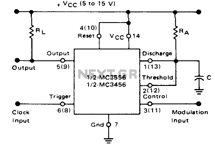
In a monostable timer circuit, such as those utilizing the 555 timer IC, the operation relies on a single stable state and a temporary unstable state. When triggered by a pulse, the timer generates a single output pulse of a defined duration. The width of this output pulse is primarily determined by the time constant formed by the resistor-capacitor (RC) network connected to the timing capacitor.
In this configuration, pin 3 serves as the control voltage input, allowing for dynamic adjustment of the threshold voltage that dictates when the timer resets. By varying the voltage at pin 3, the effective threshold voltage can be modified, thus altering the charge time of the capacitor. This adjustment leads to a change in the output pulse width, enabling applications such as pulse width modulation (PWM) where precise control over the pulse duration is required.
The ability to apply a modulating signal to pin 3 introduces an additional layer of flexibility. This signal can be derived from various sources, such as a potentiometer, another waveform generator, or a digital control signal, allowing for real-time modulation of the output pulse width. This feature is particularly useful in applications where the timing characteristics need to adapt to varying conditions, such as in motor speed control, light dimming, or audio signal processing.
The overall functionality of the monostable timer in this context emphasizes the importance of the RC network and control voltage manipulation, showcasing its versatility in electronic design for a range of applications requiring precise timing control.if the timer is triggered with a continuous pulse train in the monostable mode of operation, the charge time of the capacitor can be varied by changing the control voltage at pin 3 In this manner, the output pulse width can be modulated by applying a modulating signal that controls the threshold voltage. 🔗 External reference
Related Circuits
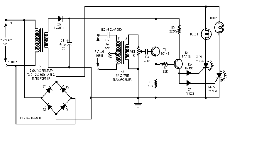
Audio Light Modulator. Audio light modulation enhances the enjoyment of music during events held at home or outdoors. Presented here is a straightforward circuit for this purpose. The audio light modulator circuit is designed to synchronize light effects with audio...
The TDA3567 is a monolithic integrated decoder designed for the NTSC color television standards. It incorporates all the necessary functions for the demodulation of NTSC signals. Additionally, it features a luminance amplifier and an RGB matrix amplifier. These amplifiers...
The RF modulator is a crucial component in televisions, VCRs, satellite receivers, format converters, home computers, and gaming consoles. This circuit is straightforward, stable, and easy to construct, allowing for seamless integration with various circuit boards. The schematic diagram...
As the number of stations increased and the power levels also rose, receiver performance had to be enhanced. The pentagrid converter, such as the 6BE6 tube (British EK90 valve), was introduced, which was optimized for mixer performance. This included...
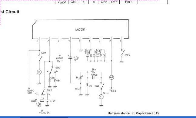
The LA7051 is a video and audio signal processor integrated circuit (IC) designed for UHF band RF modulation. It performs functions such as audio frequency modulation, video clamping, and white clipping. The LA7051 IC is engineered to facilitate the modulation...
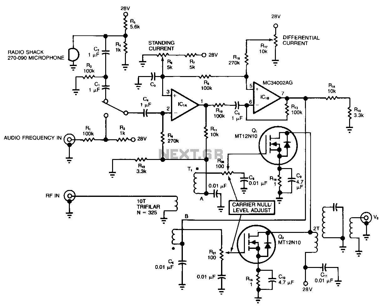
Power MOSFETs provide high power gain at both audio and radio frequencies, making them valuable in various radio circuit designs. For RF applications, the large safe operating area of a MOSFET protects it from damage caused by reflected RF...