Quartz Crystal Oscillators
1. Piezoelectric Effect and Crystal Resonance
1.1 Piezoelectric Effect and Crystal Resonance
Fundamentals of the Piezoelectric Effect
The piezoelectric effect is a reversible electromechanical coupling where certain crystalline materials generate an electric charge in response to applied mechanical stress (direct piezoelectric effect), or conversely, deform under an applied electric field (converse piezoelectric effect). In quartz crystals (SiO2), this arises from the asymmetric charge distribution within its trigonal crystal lattice structure.
For a quartz crystal plate cut along specific crystallographic axes (typically AT-cut or BT-cut), the stress-charge relationship is governed by:
where T is stress, S is strain, E is electric field, D is electric displacement, c is elastic stiffness, e is piezoelectric coefficient, and ϵ is permittivity.
Mechanical Resonance in Quartz Crystals
When an AC voltage is applied across electrodes on a properly oriented quartz blank, the converse piezoelectric effect induces thickness-shear vibrations. The crystal behaves as a high-Q mechanical resonator with resonant frequencies determined by:
where n is harmonic mode (1 for fundamental), t is thickness, c66 is stiffness coefficient for shear modes (~2.947×10¹⁰ N/m2 for AT-cut quartz), and Ï is density (2650 kg/m3).
Equivalent Electrical Model
The electromechanical behavior is commonly represented by the Butterworth-Van Dyke equivalent circuit:
Where:
- C0: Static capacitance from electrodes (~1-5pF)
- Lm, Cm, Rm: Motional arm representing mechanical resonance (typical values: mH, fF, Ω range)
The series resonant frequency occurs when:
Frequency-Temperature Characteristics
AT-cut crystals exhibit a cubic frequency-temperature relationship:
with typical coefficients a ≈ 0 and b ≈ 0.034 ppm/°C3 near 25°C, yielding excellent stability over wide temperature ranges.
Practical Considerations
Key parameters affecting oscillator performance include:
- Q-factor: Typically 104-106 for quartz, enabling frequency stability to 0.1 ppm
- Aging: Long-term frequency drift due to mass transfer or lattice defects (~0.5 ppm/year)
- Drive level: Excessive current causes nonlinear effects and frequency jumps
1.2 Crystal Cut and Frequency Determination
The frequency of a quartz crystal oscillator is fundamentally determined by its mechanical properties and the crystallographic orientation in which it is cut. The relationship between the crystal's physical dimensions, elastic constants, and resonant frequency is governed by the piezoelectric effect and the wave equation for anisotropic solids.
Crystallographic Orientation and Common Cuts
Quartz belongs to the trigonal crystal system (point group 32) and exhibits anisotropic elastic properties. The orientation of the cut relative to the crystallographic axes determines the vibrational mode and temperature stability:
- AT-cut: The most common cut, with an angle of 35°15' from the Z-axis. Provides excellent frequency stability over a wide temperature range (-40°C to +85°C) due to its turnover point near room temperature.
- BT-cut: Cut at -49° from the Z-axis. Has a higher frequency-temperature turnover point, making it suitable for higher temperature applications.
- SC-cut (Stress Compensated): A doubly rotated cut (34°18' and 21°55') that minimizes stress-induced frequency shifts, used in precision OCXOs.
Frequency Determination by Thickness Shear Mode
For AT-cut crystals operating in the thickness shear mode (TSM), the fundamental resonant frequency f is inversely proportional to the thickness t:
where N is the frequency constant, approximately 1.67 MHz·mm for AT-cut quartz. The frequency constant varies slightly with cut angle due to changes in the effective elastic stiffness c'66:
where Ï is the density of quartz (2650 kg/m³). The effective stiffness is a function of the rotation angles and the original elastic constants cij of quartz.
Overtone Operation and Harmonic Frequencies
Crystals can operate at odd harmonics (3rd, 5th, etc.) of the fundamental frequency. The overtone frequency fn is given by:
where n is the overtone order (odd integer), f1 is the fundamental frequency, and C1 is a correction factor accounting for energy trapping effects.
Temperature Dependence and Frequency Stability
The frequency-temperature relationship for AT-cut crystals follows a cubic polynomial:
where T0 is the reference temperature (typically 25°C), and coefficients a, b, c depend on the exact cut angle. For the standard AT-cut:
- a ≈ 0.0 ppm/°C (designed for zero first-order coefficient at turnover)
- b ≈ -0.04 ppm/°C²
- c ≈ -4×10â»â¸ ppm/°C³
Manufacturing Tolerances and Frequency Adjustment
Final frequency adjustment is achieved through:
- Ion milling: Precisely removes material to increase frequency
- Electrode mass loading: Adding conductive material decreases frequency
- Laser trimming: For fine adjustment of high-precision crystals
The frequency tolerance is typically specified in parts per million (ppm) and depends on the manufacturing process and subsequent aging effects, which are minimized through proper sealing and stress relief in the crystal package.
Equivalent Circuit Model of a Quartz Crystal
The electrical behavior of a quartz crystal resonator can be accurately represented by an equivalent circuit model, which captures its piezoelectric properties and resonant characteristics. This model is essential for analyzing oscillator stability, frequency response, and impedance characteristics.
Motivation for the Equivalent Circuit
Quartz crystals exhibit electromechanical resonance due to the piezoelectric effect, where mechanical vibrations couple to electrical signals. The equivalent circuit abstracts this behavior into lumped electrical components, enabling analysis using standard circuit theory. This approach is critical for designing stable oscillators and filters.
Fundamental Components
The Butterworth-Van Dyke model is the most widely used equivalent circuit, consisting of:
- Motional arm (L1, C1, R1) - Represents the mechanical resonance
- Shunt capacitance (C0) - Accounts for electrode and package capacitance
Series and Parallel Resonance
The circuit exhibits two distinct resonant frequencies:
Series resonance occurs when the motional arm impedance is minimized. The parallel resonant frequency includes C0:
Quality Factor (Q) Considerations
The quality factor quantifies energy storage versus dissipation:
Typical quartz crystals achieve Q factors exceeding 105, explaining their exceptional frequency stability compared to LC circuits.
Practical Implications
This model explains several observed phenomena:
- Frequency pulling effects from load capacitance variations
- Aging characteristics due to parameter drift
- Temperature dependence of resonant frequencies
- Spurious responses from overtone modes
Modern network analyzers can directly measure these parameters, enabling precise oscillator design. The model also forms the basis for SPICE simulations of crystal oscillator circuits.
2. Pierce Oscillator
2.1 Pierce Oscillator
The Pierce oscillator is a widely used configuration for quartz crystal oscillators due to its simplicity, stability, and low component count. It operates as a series-resonant circuit, leveraging the crystal's high Q-factor to maintain precise frequency control. The topology consists of an inverting amplifier, the crystal resonator, and two load capacitors forming a feedback network.
Circuit Topology and Operating Principle
The basic Pierce oscillator consists of:
- An inverting amplifier (typically a CMOS inverter or transistor-based stage).
- A quartz crystal (XTAL) acting as the frequency-determining element.
- Two load capacitors (C1 and C2) forming a capacitive voltage divider.
- A feedback resistor (Rf) to bias the amplifier in its linear region.
The crystal operates in its inductive region, creating a 180° phase shift when combined with the inverting amplifier, satisfying the Barkhausen criterion for oscillation. The load capacitors adjust the effective capacitance seen by the crystal, slightly pulling the resonant frequency.
Mathematical Analysis
The oscillation frequency f is determined by the crystal's series resonance and the load capacitance CL:
where:
- fs is the crystal's series resonant frequency,
- Cm is the motional capacitance,
- C0 is the shunt capacitance,
- CL is the effective load capacitance, given by:
Cstray accounts for parasitic capacitances from PCB traces and amplifier input/output. The gain condition for sustained oscillation is:
where gm is the amplifier's transconductance and RESR is the crystal's equivalent series resistance.
Practical Design Considerations
Load Capacitance: Mismatch between the designed CL and the crystal's specified load capacitance leads to frequency deviation. Typical values range from 12 pF to 32 pF.
Startup Time: Governed by the loop gain and crystal's Q-factor. Higher Q increases stability but slows startup. A gain margin of 5–10× ensures reliable oscillation.
Amplifier Selection: CMOS inverters (e.g., 74HC04) are common, biased near their linear region with Rf (1–10 MΩ). For low-phase-noise applications, discrete JFET or bipolar amplifiers are preferred.
Stability and Phase Noise
The Pierce oscillator's phase noise L(f) follows Leeson's model:
where F is the amplifier noise figure, QL is the loaded Q, and fc is the flicker noise corner frequency. Reducing Cstray and optimizing QL minimize phase noise.
Applications
- Microcontroller Clocks: Low-power variants drive CPUs (e.g., 32.768 kHz for RTCs).
- RF Systems: Stable LO references in radios and synthesizers.
- Precision Instruments: High-Q crystals enable atomic clocks and frequency standards.
2.2 Colpitts Oscillator
The Colpitts oscillator is a widely used LC oscillator topology that employs a capacitive voltage divider for feedback. Its design is particularly suited for high-frequency applications, including crystal oscillator circuits, due to its stable oscillation characteristics and ease of implementation.
Basic Operation and Circuit Configuration
The Colpitts oscillator consists of an active amplifying device (typically a bipolar junction transistor (BJT), field-effect transistor (FET), or operational amplifier), a resonant LC tank circuit, and a feedback network formed by a capacitive voltage divider. The oscillation frequency is primarily determined by the inductance L and the series combination of capacitors C1 and C2.
where Ceq is the equivalent capacitance of the series combination:
Barkhausen Criterion and Feedback Analysis
For sustained oscillations, the Colpitts oscillator must satisfy the Barkhausen criterion, requiring:
- The loop gain must be at least unity (|Aβ| ≥ 1).
- The phase shift around the loop must be an integer multiple of 360°.
The feedback factor β is determined by the capacitive divider:
The amplifier must provide sufficient gain to compensate for the feedback attenuation. For a BJT-based Colpitts oscillator, the small-signal voltage gain Av should satisfy:
Practical Implementation with Quartz Crystals
When used in crystal oscillator configurations, the Colpitts topology replaces the inductor L with a quartz crystal, which behaves as a high-Q resonant element. The crystal operates in its parallel resonant mode, where it presents an inductive reactance to complete the LC tank circuit.
The modified oscillation frequency is governed by the crystal's motional parameters:
where Lm is the motional inductance of the crystal.
Advantages and Limitations
Advantages:
- High frequency stability due to the crystal's high Q factor.
- Simple design with minimal components.
- Low phase noise, making it suitable for RF applications.
Limitations:
- Sensitivity to load capacitance variations, requiring careful tuning.
- Limited tuning range compared to other oscillator topologies.
Design Considerations
Key parameters to optimize in a Colpitts crystal oscillator include:
- Capacitor ratio (C2/C1): Affects feedback strength and loop gain.
- Bias conditions: Must ensure the active device operates in the correct region for amplification.
- Load capacitance: Must match the crystal's specified load for accurate frequency control.
Modern implementations often use CMOS inverters or op-amps for improved stability and lower power consumption, particularly in integrated circuits.
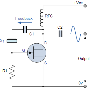
2.3 Clapp Oscillator
The Clapp oscillator, a refinement of the Colpitts oscillator, is widely used in high-frequency applications due to its superior frequency stability and low phase noise. Its distinguishing feature is the addition of a series inductor-capacitor (LC) tank circuit in the feedback path, which enhances frequency control and reduces susceptibility to parasitic capacitances.
Circuit Configuration and Operating Principle
The Clapp oscillator consists of an active device (typically a BJT or FET), a parallel LC tank circuit, and a capacitive voltage divider for feedback. Unlike the Colpitts oscillator, the Clapp variant includes an additional capacitor (C3) in series with the inductor (L), forming a resonant network that dominates the oscillation frequency. The feedback ratio is determined by capacitors C1 and C2, while C3 minimizes the influence of transistor parasitics.
Frequency Stability and Design Considerations
The Clapp oscillator's improved stability arises from the series LC network's high impedance at resonance, which reduces the impact of transistor nonlinearities. Key design parameters include:
- Q-factor optimization: The inductor L must exhibit low losses to maximize the tank circuit's quality factor (Q).
- Capacitor selection: C3 should be significantly smaller than C1 and C2 to dominate the resonant frequency.
- Bias stability: Active device biasing must ensure consistent transconductance to sustain oscillations.
Practical Applications
Clapp oscillators are favored in:
- VHF/UHF signal sources: Their low phase noise makes them ideal for communication systems.
- Frequency synthesizers: The high stability supports precise frequency generation.
- Test equipment: Used in signal generators and spectrum analyzers for clean reference signals.
Comparison with Colpitts and Hartley Oscillators
While the Colpitts oscillator relies solely on capacitive feedback, the Clapp topology's series LC network provides better immunity to component tolerances. The Hartley oscillator, using inductive feedback, suffers from higher phase noise due to inductor losses, making the Clapp configuration preferable for stable high-frequency operation.
where F is the noise figure, k is Boltzmann's constant, T is temperature, Q is the quality factor, and Posc is the oscillation power.
Design Example
For a 10 MHz Clapp oscillator:
- Select L = 2.5 µH (Q > 100).
- Choose C1 = 100 pF, C2 = 100 pF, and C3 = 10 pF to ensure frequency dominance by C3.
- Verify loop gain βAv > 1, where β = C1/(C1 + C2).
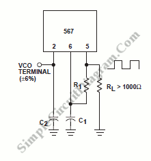
Voltage-Controlled Crystal Oscillator (VCXO)
A Voltage-Controlled Crystal Oscillator (VCXO) is a type of oscillator where the output frequency can be finely tuned by applying an external control voltage. Unlike standard crystal oscillators, which operate at a fixed frequency determined by the mechanical resonance of the quartz crystal, a VCXO incorporates a voltage-dependent reactance element (typically a varactor diode) to enable frequency modulation.
Operating Principle
The frequency of a VCXO is governed by the series resonance of the quartz crystal, modified by the capacitive load imposed by the varactor diode. The control voltage (Vctrl) alters the varactor's junction capacitance (Cj), which in turn shifts the oscillator's resonant frequency. The relationship between the control voltage and the output frequency is given by:
where:
- f0 is the natural resonant frequency of the crystal,
- C0 is the shunt capacitance of the crystal,
- CL is the fixed load capacitance,
- Cj(Vctrl) is the voltage-dependent capacitance of the varactor.
Varactor Diode Characteristics
The varactor diode's capacitance varies inversely with the applied reverse bias voltage, following the equation:
where:
- Cj0 is the zero-bias junction capacitance,
- Vφ is the built-in potential (typically ~0.7V for silicon),
- n is the grading coefficient (ranging from 0.3 to 0.5 for abrupt junctions).
Frequency Pulling Range
The pulling range of a VCXO defines the maximum frequency deviation achievable with the control voltage. It is expressed in parts per million (ppm) and is determined by:
where Cj,min and Cj,max are the varactor capacitances at the minimum and maximum control voltages, respectively.
Phase Noise Considerations
VCXOs exhibit higher phase noise compared to fixed-frequency oscillators due to the added noise from the varactor diode and control voltage source. The phase noise (L(f)) can be modeled as:
where:
- F is the noise figure,
- k is Boltzmann's constant,
- T is temperature,
- Psig is the signal power,
- QL is the loaded quality factor,
- fc is the flicker noise corner frequency.
Applications
VCXOs are widely used in:
- Clock recovery circuits in digital communication systems,
- Phase-locked loops (PLLs) for frequency synthesis,
- Jitter attenuation in high-speed serial links,
- Frequency modulation in RF transmitters.
Design Trade-offs
Key design considerations include:
- Linearity – Ensuring a predictable frequency vs. voltage response,
- Temperature stability – Compensating for varactor drift,
- Load capacitance matching – Minimizing frequency deviations due to external circuit variations.
3. Load Capacitance and Frequency Stability
3.1 Load Capacitance and Frequency Stability
The resonant frequency of a quartz crystal oscillator is highly sensitive to the load capacitance (CL) connected across its terminals. This dependency arises because the crystal operates as a high-Q resonant circuit, where even small changes in the load impedance can perturb the oscillation frequency. The relationship between load capacitance and frequency deviation is derived from the crystal's equivalent circuit model.
Equivalent Circuit and Load Capacitance Effects
A quartz crystal's electrical behavior is modeled by the Butterworth-Van Dyke equivalent circuit, consisting of a series RLC branch (motional parameters: L1, C1, R1) in parallel with a shunt capacitance (C0). When external load capacitance CL is added, the effective capacitance seen by the crystal becomes:
This modifies the crystal's parallel resonant frequency (fp), given by:
where fs is the series resonant frequency. For small perturbations, the fractional frequency shift (Δf/f) due to CL is approximated by:
Practical Implications for Frequency Stability
In oscillator circuits, CL is typically specified by the crystal manufacturer (e.g., 8 pF, 12 pF, 18 pF). Deviations from this value introduce frequency errors. For example, a 1 pF mismatch in a 10 MHz crystal with C1 = 20 fF and C0 = 5 pF causes a shift of:
To mitigate this, designers must:
- Match CL precisely to the crystal's datasheet value using trimmer capacitors or fixed ceramic capacitors with tight tolerances (e.g., ±0.1 pF).
- Minimize parasitic capacitances in PCB traces and oscillator circuitry, which add to CL.
- Use low-impedance drive circuits to reduce the impact of load variations.
Temperature and Aging Considerations
Frequency stability is further influenced by temperature coefficients and long-term aging. The load capacitance sensitivity (Δf/ΔCL) is temperature-dependent due to changes in C1 and C0 with thermal drift. For AT-cut crystals, this effect is minimized near the turnover temperature (typically 25°C), but deviations exacerbate CL-induced instability.
Aging, caused by stress relaxation in the crystal lattice, alters C1 over time (typically 1–5 ppm/year). This shifts the CL-frequency curve, requiring periodic recalibration in precision applications like atomic clocks or GPS receivers.
3.2 Temperature Compensation Techniques
Thermal Effects on Quartz Crystal Frequency
The resonant frequency of a quartz crystal is highly sensitive to temperature variations due to the anisotropic thermal expansion of the crystal lattice and changes in the elastic constants. The frequency-temperature relationship is typically modeled by a third-order polynomial:
where a, b, and c are coefficients specific to the crystal cut (e.g., AT-cut, SC-cut), T is the operating temperature, and T0 is the reference temperature (usually 25°C). For AT-cut crystals, the dominant term is the quadratic component (b), resulting in a parabolic frequency-temperature curve.
Passive Temperature Compensation
Passive techniques involve modifying the oscillator circuit to counteract the crystal's frequency drift without active control. The most common method is the use of temperature-compensating capacitors (TCCs) or varactor diodes with a tailored temperature coefficient. The load capacitance CL is adjusted as:
where α is chosen to offset the crystal's frequency-temperature coefficient. This method is limited to narrow temperature ranges (±10°C) but is cost-effective for consumer electronics.
Oven-Controlled Crystal Oscillators (OCXOs)
For high-stability applications, OCXOs maintain the crystal at a constant temperature (typically 70–80°C) using a proportional-integral-derivative (PID) controller. The oven's thermal time constant τ and power dissipation P are critical:
where m is the crystal mass, c is specific heat, h is the heat transfer coefficient, and A is the surface area. OCXOs achieve frequency stabilities of ±0.01 ppm but consume significant power (1–5 W).
Digital Temperature Compensation (DTCXO)
Modern DTCXOs use a temperature sensor (e.g., thermistor or IC) and a lookup table (LUT) to apply corrective tuning via a digital-to-analog converter (DAC). The frequency correction Δf is computed as:
where kn are polynomial coefficients stored in non-volatile memory. Advanced implementations use piecewise linear approximation or neural networks for nonlinear compensation, achieving ±0.1 ppm stability over −40°C to +85°C.
Microcomputer-Compensated Crystal Oscillators (MCXO)
MCXOs integrate a microcontroller to dynamically adjust compensation parameters based on real-time temperature data and hysteresis modeling. The algorithm minimizes the residual error:
This technique is used in precision timing systems like GPS receivers and telecom base stations, with stabilities reaching ±0.05 ppm.
Case Study: TCXO in 5G NR Synchronization
In 5G New Radio (NR), TCXOs with ±0.28 ppm stability are employed to meet 3GPP's stringent synchronization requirements (≤±1.5 μs time error). A typical implementation uses a ΣΔ-modulated DAC to fine-tune the crystal load capacitance, compensating for rapid temperature gradients induced by RF power amplifiers.
Phase Noise and Jitter in Oscillators
Fundamentals of Phase Noise
Phase noise quantifies the short-term frequency instability of an oscillator, expressed as the power spectral density (PSD) of phase fluctuations. It is typically measured in dBc/Hz at a specified offset frequency from the carrier. The Leeson model provides a foundational framework for phase noise analysis in feedback oscillators:
where fm is the offset frequency, F is the noise figure, k is Boltzmann’s constant, T is temperature, P0 is the carrier power, f0 is the oscillator frequency, QL is the loaded quality factor, and fc is the flicker noise corner frequency.
Jitter: Time-Domain Manifestation of Phase Noise
Jitter represents the time-domain counterpart of phase noise, describing the deviation of zero-crossing points from their ideal positions. For a stationary process, the root-mean-square (RMS) jitter σt relates to phase noise through integration:
where Ï„ is the measurement interval and fL, fH define the integration bandwidth. In practical systems, jitter is categorized as:
- Period jitter: Cycle-to-cycle variation in period duration
- Cycle-to-cycle jitter: Difference between consecutive periods
- Long-term jitter: Accumulated deviation over multiple cycles
Crystal Oscillator-Specific Considerations
Quartz crystal oscillators exhibit superior phase noise performance due to their high Q factors (typically 104–106). The modified Leeson equation for crystal oscillators incorporates the resonator’s motional parameters:
where Rm and Lm are the motional resistance and inductance of the crystal. The 1/f3 region dominates close to the carrier, while thermal noise creates a 1/f2 slope at higher offsets.
Measurement Techniques
Phase noise characterization employs either:
- Spectrum analyzer methods: Direct PSD measurement with correction for instrument noise floor
- Phase detector techniques: Mixer-based systems comparing DUT against a reference
For jitter measurement, time-interval analyzers (TIAs) or sampling oscilloscopes provide picosecond-level resolution. The Allan variance σy(τ) serves as a time-domain metric for stability analysis:
Design Tradeoffs and Optimization
Key design parameters affecting phase noise include:
| Parameter | Phase Noise Impact | Practical Constraint |
|---|---|---|
| Q factor | ∠1/Q2 | Crystal size, cost |
| Carrier power | ∠1/P0 | Power dissipation |
| Flicker corner | Low-frequency noise | Active device selection |
Advanced techniques like substrate biasing and differential topologies reduce flicker noise contribution from active devices. In MEMS oscillators, nonlinear stabilization methods can improve close-in phase noise by 10–15 dB.
System-Level Implications
In communication systems, phase noise degrades error vector magnitude (EVM) and adjacent channel leakage ratio (ACLR). For clock distribution networks, jitter causes timing margin reduction following:
Radar systems particularly suffer from phase noise-induced false targets, as the noise floor determines the minimum detectable signal level.
4. Clock Generation in Digital Systems
4.1 Clock Generation in Digital Systems
Fundamentals of Clock Signal Generation
The stability and precision of clock signals in digital systems are paramount, as they synchronize operations across processors, memory interfaces, and communication buses. Quartz crystal oscillators dominate this application due to their exceptional frequency stability, typically achieving tolerances of ±10 to ±100 ppm. The piezoelectric effect in quartz crystals generates a resonant frequency when an alternating electric field is applied, governed by the crystal's mechanical dimensions and cut.
Mathematical Basis of Crystal Resonance
The resonant frequency f of a quartz crystal is determined by its thickness t and the material's stiffness coefficient c. For an AT-cut crystal (common in digital systems), the fundamental frequency is:
where Ï is the density of quartz (2.65 g/cm³). For harmonic modes, odd integer multiples (3rd, 5th, etc.) are used, though with diminishing electromechanical coupling efficiency.
Oscillator Circuit Topologies
Three primary configurations are employed in digital systems:
- Pierce Oscillator: Most common in CMOS systems, using an inverter as gain element with capacitive feedback (C1, C2) setting the load capacitance.
- Colpitts Oscillator: Uses a tapped capacitor network, favored for higher frequencies (>30 MHz).
- Clapp Oscillator: Variant with series-tuned LC tank, providing improved frequency pulling range.
Phase Noise and Jitter Considerations
Clock integrity is quantified by phase noise (£(f)) and jitter (σt). For a 10 MHz crystal oscillator with Q=105, the single-sideband phase noise follows:
where F is the noise figure (typically 3-6 dB for CMOS amplifiers) and Psig is the oscillation power.
Temperature Compensation Techniques
Advanced digital systems employ either:
- TCXO (Temperature-Compensated Crystal Oscillator): Uses analog compensation network with thermistors to adjust load capacitance.
- OCXO (Oven-Controlled Crystal Oscillator): Maintains crystal at constant temperature (±0.01°C) for ultra-stable references.
Modern Implementation: MEMS vs. Quartz
While MEMS oscillators offer advantages in shock resistance (200,000g vs. 5,000g for quartz), their phase noise performance at 1 MHz offset remains 10-20 dB worse than equivalent quartz devices. The Allan deviation for a high-end quartz oscillator reaches 10-12 at Ï„=1s averaging time, versus 10-9 for MEMS.
4.2 Frequency Synthesis and RF Applications
Phase-Locked Loops and Frequency Multiplication
Quartz crystal oscillators serve as stable reference sources in phase-locked loop (PLL) frequency synthesizers, enabling precise frequency multiplication. The PLL compares the phase of a voltage-controlled oscillator (VCO) output with the crystal reference using a phase detector, generating an error voltage that locks the VCO to an integer multiple of the reference frequency.
where N is the division ratio of the feedback counter. Advanced fractional-N synthesizers achieve finer resolution by dynamically modulating N between integer values, producing an effective non-integer multiplication factor.
Direct Digital Synthesis (DDS) Systems
High-stability crystal references enable precise direct digital synthesis, where a numerically controlled oscillator (NCO) generates programmable output frequencies through phase accumulation and digital-to-analog conversion. The spectral purity of the crystal oscillator directly impacts DDS phase noise performance, particularly in RF applications where close-in phase noise is critical.
where fclk is the crystal reference frequency. Modern DDS chips achieve sub-Hz frequency resolution with jitter performance directly tied to the reference oscillator's quality factor (Q).
RF Upconversion and Heterodyne Systems
In radio transceivers, crystal oscillators provide the local oscillator (LO) signals for mixing operations. The LO stability determines receiver selectivity and transmitter spectral compliance. Common architectures include:
- Superheterodyne receivers: Crystal-referenced LOs convert RF signals to fixed intermediate frequencies
- Image-reject mixers: Quadrature signals derived from crystal oscillators enable sideband cancellation
- Digital IF systems: High-speed crystal clocks sample intermediate frequencies directly
Phase noise requirements become particularly stringent in dense RF environments, where oscillator noise floors below -160 dBc/Hz are often necessary to prevent reciprocal mixing.
Microwave Frequency Generation
Fundamental-mode crystals (typically ≤50 MHz) are multiplied into microwave bands using step-recovery diodes or active multiplier chains. The multiplication process preserves the crystal's frequency stability while introducing phase noise degradation proportional to 20log10(N), where N is the multiplication factor:
Modern surface-acoustic-wave (SAW) stabilized oscillators and dielectric resonator oscillators (DROs) often replace multiplier chains above 2 GHz, offering improved phase noise performance.
Atomic Clock References
In precision timing applications, quartz oscillators are disciplined to atomic references (rubidium, cesium, or hydrogen maser standards) through digital servo systems. The quartz provides short-term stability while the atomic reference corrects long-term drift, achieving parts in 1013 accuracy. This hybrid approach is standard in GPS timing receivers and telecommunications network synchronization.
where σy(τ) is the Allan deviation, Q is the loaded quality factor, and P0 is the oscillator power.
4.3 Timekeeping and Real-Time Clocks
Fundamentals of Crystal-Based Timekeeping
Quartz crystal oscillators serve as the backbone of precision timekeeping in modern electronics due to their exceptional frequency stability. When a voltage is applied, the piezoelectric effect causes the crystal to vibrate at its resonant frequency, typically 32.768 kHz for real-time clocks (RTCs). This frequency is chosen because it is a power of two (215), allowing simple binary division to derive a 1 Hz signal for seconds counting.
where fxtal is the crystal frequency and n is the number of divider stages.
Temperature Compensation and Stability
The frequency stability of a quartz oscillator is affected by temperature variations, following a parabolic relationship described by:
where a, b, and c are coefficients specific to the crystal cut (typically AT-cut for RTCs), and T0 is the turnover temperature.
Temperature-compensated crystal oscillators (TCXOs) and oven-controlled crystal oscillators (OCXOs) employ active compensation techniques to mitigate these effects, achieving stabilities of ±0.5 ppm to ±0.01 ppm over industrial temperature ranges.
Real-Time Clock (RTC) Circuit Design
A typical RTC circuit consists of:
- A 32.768 kHz tuning-fork crystal
- An oscillator circuit with load capacitors (CL)
- A divider chain to generate 1 Hz pulses
- Battery backup circuitry
The load capacitance must match the crystal's specified value (typically 6-12.5 pF) to ensure accurate frequency:
where C1 and C2 are the external capacitors and Cstray accounts for PCB parasitics.
Advanced RTC Implementations
Modern RTC ICs integrate:
- Automatic battery switchover
- Digital temperature compensation
- I2C or SPI interfaces
- Timestamped alarm functions
For ultra-low-power applications, the oscillator's transconductance (gm) must satisfy:
where C0 is the crystal shunt capacitance and Resr is the equivalent series resistance.
Practical Considerations
Board layout significantly impacts RTC performance:
- Keep crystal traces short (<5 mm) and symmetrical
- Implement a ground plane beneath the crystal
- Use guard rings to reduce EMI pickup
- Select capacitors with tight tolerances (±5% or better)
For mission-critical applications, the Allan deviation (σy(τ)) quantifies frequency stability over time:
where M is the number of frequency measurements and Ï„ is the averaging time.
5. Common Failure Modes and Diagnostics
5.1 Common Failure Modes and Diagnostics
Frequency Drift and Aging
Quartz crystals experience gradual frequency shifts due to material aging, where impurities migrate through the lattice structure. The frequency drift follows:
where A represents the aging constant (typically 0.5–5 ppm/year for AT-cut crystals), B is the contamination factor, and t is time. Industrial applications mitigate this through oven-controlled oscillators (OCXOs) with aging rates below 0.1 ppb/day.
Mechanical Stress Fractures
Excessive mechanical shock (≥ 5,000 G) can fracture the crystal blank, particularly at the nodal points where stress concentrates. Diagnostic indicators include:
- Abrupt frequency jumps exceeding 100 ppm
- Increased phase noise floor (> -140 dBc/Hz at 1 kHz offset)
- Harmonic distortion spikes at 3rd and 5th overtones
Electromigration in Electrodes
High current density (> 10 μA/μm²) causes gold electrode thinning, increasing equivalent series resistance (ESR). The failure progression follows:
where J is current density, T is temperature, and α is the material constant (3.2×10â»â´ for gold). Spectroscopic analysis reveals this through increased motional inductance (L1) in impedance measurements.
Outgassing in Hermetic Seals
Failed seals allow atmospheric contamination, causing:
- Hydrogen absorption (frequency decrease up to 200 ppm)
- Water vapor adsorption (Q-factor degradation by 40–60%)
Helium leak testing at 10â»â¹ atm·cc/sec sensitivity detects seal failures before operational degradation.
Thermal Hysteresis Effects
Non-repeatable frequency-temperature characteristics emerge from:
- Anisotropic stress in mounting adhesives (Δf/f ≈ 2–8 ppm)
- Crystal lattice dislocations (particularly in SC-cut crystals)
Diagnostic thermal cycling (-55°C to +125°C) reveals hysteresis loops exceeding 0.5 ppm in compromised units.
Ionizing Radiation Damage
Space applications require radiation-hardened crystals. Gamma exposure (> 10 krad) induces:
where K is the radiation sensitivity coefficient (0.03–0.15 ppm/rad for swept quartz), ϕ is flux, and Ea is activation energy (0.35 eV for aluminum impurities).
Diagnostic Techniques
Advanced characterization methods include:
- Network analysis: Measures impedance circle deviations indicating ESR changes
- Laser interferometry: Detects micro-deformations in crystal blanks
- X-ray topography: Visualizes lattice dislocations in real-time
5.2 Improving Frequency Accuracy and Stability
The frequency accuracy and stability of a quartz crystal oscillator are critical for applications requiring precise timing, such as telecommunications, atomic clocks, and navigation systems. Several factors influence these parameters, including temperature variations, aging, and circuit design. Below, we explore advanced techniques to mitigate these effects.
Temperature Compensation
Quartz crystals exhibit a frequency-temperature dependency described by a third-order polynomial approximation:
where f0 is the nominal frequency, T0 is the reference temperature (typically 25°C), and α, β, γ are material-specific coefficients. To counteract this drift, two primary methods are employed:
- Temperature-Compensated Crystal Oscillators (TCXOs): These use analog or digital compensation networks that adjust the load capacitance based on a temperature sensor's feedback.
- Oven-Controlled Crystal Oscillators (OCXOs): The crystal is maintained at a constant elevated temperature (e.g., 75°C) to minimize thermal gradients, achieving stabilities below ±0.01 ppm.
Aging Mitigation
Aging refers to the gradual frequency shift caused by mechanical stress relaxation, contamination, and lattice defects. The aging rate is empirically modeled as:
where A and B are constants, and t is time. Strategies to reduce aging include:
- Pre-aging: Subjecting the crystal to elevated temperatures (>85°C) for extended periods to accelerate stress relaxation before deployment.
- Hermetic Sealing: Using cold-weld or ceramic enclosures to prevent outgassing and contamination.
Phase Noise Reduction
Phase noise, a critical metric for RF applications, stems from thermal (Johnson-Nyquist) noise, flicker noise, and vibration-induced jitter. The Leeson model describes phase noise L(f) as:
where F is the noise figure, Q is the quality factor, and fc is the flicker noise corner. Practical improvements include:
- High-Q Crystals: SC-cut crystals offer Q values exceeding 1 million, reducing close-in phase noise.
- Low-Noise Amplifiers: JFET-based sustaining amplifiers minimize additive noise.
Circuit-Level Enhancements
Load capacitance (CL) variations directly impact frequency via the series resonance equation:
To stabilize CL:
- Varactor Tuning: Automatic frequency control (AFC) loops adjust CL dynamically using voltage-controlled capacitors.
- Trimming: Laser-trimmed or MEMS-adjusted capacitors compensate for initial tolerances.
5.3 Mitigating Environmental Effects
Quartz crystal oscillators are highly sensitive to environmental perturbations, including temperature fluctuations, mechanical stress, and electromagnetic interference. Advanced techniques are required to stabilize their performance under varying conditions.
Temperature Compensation Techniques
The frequency-temperature dependence of a quartz crystal follows a third-order polynomial approximation:
where f0 is the nominal frequency, T0 is the turnover temperature, and α, β, γ are material-specific coefficients. To counteract this drift:
- Oven-Controlled Crystal Oscillators (OCXOs): Maintain the crystal at a constant temperature using a precision heating element and feedback control.
- Temperature-Compensated Crystal Oscillators (TCXOs): Use analog or digital compensation networks to adjust the load capacitance dynamically.
- Microcomputer-Compensated Crystal Oscillators (MCXOs): Employ real-time frequency correction via lookup tables or polynomial fitting.
Mechanical Stress Mitigation
Mechanical strain alters the crystal's resonant frequency due to the stress-optic effect. The frequency shift Δf under applied stress σ is given by:
where K is the stress sensitivity coefficient. Countermeasures include:
- Isolation Mounting: Soft adhesives or suspension systems decouple the crystal from PCB-induced strain.
- Symmetrical Packaging: Minimizes thermal gradients and asymmetric stress distribution.
- Low-Stress Bonding: Au-Si eutectic or conductive epoxy reduces mounting-induced deformation.
Electromagnetic Interference (EMI) Shielding
High-frequency noise couples into the oscillator circuit, introducing phase jitter. The resulting timing error Δt for a sinusoidal perturbation of amplitude Vn is:
Effective shielding strategies involve:
- Faraday Cages: Conductive enclosures attenuate external RF fields.
- Twisted-Pair Traces: Reduces magnetic field coupling in differential signal lines.
- Ferrite Beads: Suppresses high-frequency common-mode currents on power rails.
Aging Compensation
Long-term frequency drift occurs due to material outgassing and electrode migration. The aging rate follows a logarithmic decay:
where A is the aging coefficient and Ï„ is the time constant. Mitigation approaches include:
- Pre-Aging: Accelerated thermal cycling stabilizes the crystal before deployment.
- Hermetic Sealing: Cold-welded metal packages prevent contamination ingress.
- Active Trim: Periodic calibration via varactor diodes or digital trimming.
For mission-critical applications, combining these techniques in hybrid architectures (e.g., DOCXO - Double Oven Crystal Oscillator) achieves sub-ppb stability.
6. Key Research Papers and Books
6.1 Key Research Papers and Books
- Low-Power Crystal and Mems Oscillators: The Experience of ... - Bookshop — Preface. List of Symbols. 1Introduction. 1.1 Applications of Quartz Oscillators. 1.2 Historical Notes. 1.3 The Book Structure. 1.4 Basics on Oscillators. 2 Quartz and MEMs Resonators. 2.1 The Quartz Crystal resonator. 2.2 Equivalent Circuit. 2.3 Figure of Merit. 2.4 Mechanical Energy and Power Dissipation. 2.5 Various Types of Quartz Resonators. 2.6 MEMs Resonators. 3 General Theory of High-Q ...
- PDF Understanding quartz crystals and oscillators - GBV — X Understanding Quartz Crystals andOscillators 2.3 QuartzCrystal Cuts 42 2.3.1 TheAT, BT,andSCCuts 42 2.4 TemperatureCharacteristics ofATCut,BTCut, andSCCut 43 2.4.1 AT-CutFrequency-Temperature Curves 43 2.4.2 BT-CutFrequency-Temperature Curves 43 2.4.3 SC-CutFrequency-Temperature Curves 43 2.5 Thickness VersusFrequencyofQuartzWafers (Blanks) 45 2.6 BechmannFrequency-Temperature Curves 47
- PDF Quartz Crystal Resonators and Oscillators for Frequency Control and ... — Quartz Crystal Resonators and Oscillators for Frequency PE: iLl Control and Timring Applications -A Tutorial PR: 62705 6. AUTHOR(S) TA: AH94 7., PERFORMING ORGANIZATION NAME(S) AND ADDRESS(ES) S. PERFORMING ORGANIZATION REPOHT NUMBER Army Research Laboratory Elecroncs SoucesDirctoateSLCET-TR-88-1 nd owe (Rev. 6.1)
- Quartz crystal resonators and oscillators for frequency control and ... — The following subjects are covered: applications of frequency standards; types of oscillators (quartz and atomic); quartz resonator properties; quartz growing, sweeping, and material characteristics; Q and its significance; resonator and oscillator stability, including aging, short-term instability, frequency vs. temperature characteristics, oscillator circuit caused instabilities, frequency ...
- Quartz Crystal Resonators and Oscillators for Frequency Control and ... — Health & Environmental Research Online (HERO) Contact Us; Print Feedback Export to File . Search: This record has one attached file: ... Save. Citation; Tags; HERO ID. 1784280 Reference Type. Technical Report Title. Quartz Crystal Resonators and Oscillators for Frequency Control and Timing Applications: A Tutorial (Revision 6.1) Author(s) Vig ...
- PDF The Designer's Guide to High-Purity Oscillators — ISBN 1-4020-7666-5 e-ISBN 0-387- 23294-X Printed on acid-free paper. 63 2005 Kluwer Academic ... to the vibrations of a quartz crystal in a wrist watch. The study of oscillators was initiated centuries ago in basic ... to address phase noise as a distinct class of noise in electronic oscillators and . Preface I try to predict it using ...
- RF Oscillators - SpringerLink — The classical method to obtain oscillations with very high frequency stability is to use a quartz crystal that electrically behaves as a very high Q resonance circuit. 6.3.1 Crystal Oscillators. A thin prism cut and lapped from a native quartz crystal is shown in Fig. 6.12.
- Quartz Crystal Resonators and Oscillators for Frequency Control and ... — An analysis has been made of the potential effects of AM-to-FM noise conversion in quartz crystal oscillators as a result of the dynamic frequency-drive sensitivity of the crystal resonator.
- UNIVERSITY OF NEVADA, RENO Introduction to Quartz Resonator Based ... — 356.875 MHz inverted-mesa etched 3rd overtone AT cut quartz resonator. It is, therefore, demonstrated that the inverted-mesa etched quartz resonator can be used in the same oscillator circuits that use the traditionally processed resonators and can enable the economical use of quartz crystal oscillators at frequencies above that which was possible
- PDF Experimental and Theoretical Study of Quartz And — The fundamental mechanical noise of the quartz tuning fork was measured and is due to thermal fluctuations at the measurement temperature (-300K) associated with the dissipation in the mechanical system and can be related to the effective resistance of the resonator
6.2 Manufacturer Datasheets and Application Notes
- PDF AN2867 Application note - STMicroelectronics — Quartz crystal properties and model AN2867 6/59 AN2867 Rev 23 1 Quartz crystal properties and model A quartz crystal is a piezoelectric device converting electric energy into mechanical energy, and vice versa. The transformation occurs at the resonant frequency. The quartz crystal can be modeled as shown in Figure 1. Figure 1. Quartz crystal model
- PDF High Performance Quartz Crystals Crystal Oscillators Qcm Sensors — QUARTZ CRYSTALS CRYSTAL OSCILLATORS QCM SENSORS www.quartzpro.com [email protected] Tel:+46-8-795 99 15 Issue date 2009-02-06 Revision date 2014-08-15 Page 3 of 3 World Class Quality and Service DETAILED SPECIFICATION FOR QCM SENSOR PART # QCM6125AgAl115-115-S PRODUCT PART NUMBER DESIGNATION AND INTERPRETATION.
- PDF Miniature - Ovenized Crystal Oscillator Series QO202 - Quintenz — The ovenized crystal oscillators are approved in the following environmental conditions: QUINTENZ Hybridtechnik GmbH Eichenstr. 15 D-82061 Neuried Tel.+49(0)89/7592252 Fax+49(0)89/7592545 - Series Recommended Soldering Profile: 0 50 100 150 200 250 300 0 60 120 Time [s]180 240 300] C ° [ e u t ar p me T >180°C 150s 20s max @ 240°C ±5°C x a m
- PDF Oscillator design guide for ST microcontrollers — Quartz crystal properties and model AN2867 6/23 Doc ID 15287 Rev 3 1 Quartz crystal properties and model A quartz crystal is a piezoelectric device transforming electric energy to mechanical energy and vice versa. The transformation occurs at the resonant frequency. The quartz crystal can be modeled as follows: Figure 1. Quartz crystal model
- Crystals - CTS Corp — High Q Quartz Resonators; Fundamental and 3 rd Overtone Crystal Designs; ... Automotive Grade Crystals and Clock Oscillators (AEC-Q200) Application Notes / Tech Briefs, Brochures / Catalogs, Guides / Tools ... Application Notes / Tech Briefs. Filters. clear all. Keywords. Frequency Stability clear. ±250 (0) ±200 (0) ±100 (15)
- PDF MULTIPLE OUTPUT LVDS SERIES Q-TECH 3.3Vdc, 1 to 12 Differential LVDS ... — 3.3Vdc, 1 to 12 Differential LVDS Pairs, Space Qualified Crystal Oscillators 15MHz to 200MHz Q-TECH CORPORATION QPDS-0115 Rev. F - December 2024 3 of 18 Level S except as modified or supplemented herein. 6.2 Approved Source of Supply Hybrid crystal oscillators shall be supplied from the manufacturer specified in "Source of Supply" below.
- (PDF) AN2867 Application note Oscillator design guide for ST ... — Quartz crystal oscillators is widely used in many types of electronics equipment for our daily life applications such as mobile communication, military, industrial measurement, an others due to its high stability clock sources. ... AN2867 Application note Oscillator design guide for ST microcontrollers Introduction Most designers are familiar ...
- PDF Fundamentals of Quartz Oscillators - LeapSecond — Crystal Structure The quartz crystal is formed from silicon and oxygen (Si02). Its charac-teristic form is a result of the unit cells by which the crystal grows. These unit cells are identical and consist of atoms arranged in a repetitive geometric pattern. Quartz crystals have a three dimen-sional geometric body (Figure 4).
- PDF AN0016.2: Oscillator Design Considerations - Silicon Labs — The EFM32 and EFR32 Wireless Gecko Series 2 crystal oscillators use a relatively low oscillation amplitude, which can lead to a lower oscillation frequency than stated as the nominal value in the crystal's data sheet. More information on this effect is given in 6.4 Fre-quency Pulling. 3.1 Timeout
- PDF "Back to Basics" - specifying quartz crystals & oscillators — Quartz Crystals and Oscillators Digital Days Webinar ... Applications Support Engineer IQD Frequency Products Ltd, UK IQD has been part of the Wurth Group since 2017 [email protected]. ... Note: you cannot measure the stray capacitance in the circuit
6.3 Online Resources and Tutorials
- PDF Understanding quartz crystals and oscillators - GBV — X Understanding Quartz Crystals andOscillators 2.3 QuartzCrystal Cuts 42 2.3.1 TheAT, BT,andSCCuts 42 2.4 TemperatureCharacteristics ofATCut,BTCut, andSCCut 43 2.4.1 AT-CutFrequency-Temperature Curves 43 2.4.2 BT-CutFrequency-Temperature Curves 43 2.4.3 SC-CutFrequency-Temperature Curves 43 2.5 Thickness VersusFrequencyofQuartzWafers (Blanks) 45 2.6 BechmannFrequency-Temperature Curves 47
- Tutorial (Quartz Crystal Resonators and Oscillators) (John R. Vig) - Scribd — The document provides a tutorial on quartz crystal resonators and oscillators used for frequency control and timing applications. It covers 10 topics including applications and requirements, quartz crystal oscillators, quartz crystal resonators, oscillator stability, quartz material properties, atomic frequency standards, oscillator comparison and specification, time and timekeeping, related ...
- Quartz Crystal Oscillator Circuits Design Handbook — Quartz Crystal Oscillator Circuits Design Handbook - Free download as PDF File (.pdf), Text File (.txt) or read online for free. ... 6-3. TRIOpE AMPLIFIER CHARACTERISTICS. 152. 6-4. Limiting Action of a Tube ... All sinusoidal electronic oscillators can be considered as consisting of a power amplifier and a network which selects a portion of ...
- Quartz Crystal Oscillator Circuits Design Handbook — Quartz Crystal Oscillator Circuits Design Handbook, D. Firth. Department of the Army Project No. 3A99-15-004. Addeddate 2016-03-04 21:17:05 Foldoutcount 0 Identifier AD460377 Identifier-ark ark:/13960/t5w70s07j Ocr ABBYY FineReader 11.0 Ocr_converted abbyy-to-hocr 1.1.7 ...
- PDF AN0016.2: Oscillator Design Considerations - Silicon Labs — Crystal oscillators Crystal oscillators use the mechanical vibration of a crystal to generate the clock signal. Due to the molecular composition of the crys-tal matter and the angle of which the crystal is cut, this type of oscillator is very precise and stable over a wide temperature range. The most commonly used crystal is the quartz crystal.
- PDF QUARTZ CRYSTALS IN THEORY AND PRACTICE - BCE SRL Importation ... — the product as a whole. The same applies to quartz crystals in electronic applications. Quartz crystals can be found in almost every electronic device with integrated time measurement, as for example watches, smartphones or microwaves. In the field of digital data processing, quartz crystals can be found even more frequently.
- PDF Oscillator Design Considerations - EEWeb — The EFM32 microcontrollers contain two crystal oscillators, one low speed (32.768 kHz) and one high speed (4-32 MHz or 4-48 MHz). ... An oscillator is an electronic circuit which generates a repetitive time-varying signal, which in this context ... Quartz crystals and ceramic resonators hold the direct piezoelectric property. This means an applied
- 6.3 Quartz crystal oscillators - Newnes Radio and RF Engineering Pocket ... — This space intentionally left blank. - Selection from Newnes Radio and RF Engineering Pocket Book, 3rd Edition [Book]
- PDF Chapter 6 Oscillator Circuits - Wilfrid Laurier University — 6.2 Background 6-3 Figure 6.2: Crystal Equivalent Circuit Crystal Oscillator You can see that the previous circuit lacks precision. Another way to design an oscillator is to set up a resonant circuit in the feedback network. In order to increase the precision, the quality factor, Q, of the resonant circuit must be large.
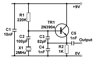
- How do I use a quartz crystal in an oscillator? - Electrical ... — Voltage can be something within the operating range of the IC, such as 5V. You may need to add a series resistor to limit the crystal drive (you need to check the crystal datasheet for manufacturer recommendations) Here is a circuit with typical component values: Note the series R mentioned above.