RC Circuits
1. Definition and Basic Components
Definition and Basic Components
An RC circuit consists of a resistor (R) and a capacitor (C) connected in series or parallel, forming a first-order linear system governed by differential equations. These circuits exhibit transient behavior when subjected to step inputs, making them fundamental in signal processing, filtering, and timing applications.
Core Components
The two primary elements of an RC circuit are:
- Resistor (R): A passive component that opposes current flow, dissipating energy as heat according to Ohm's Law (V = IR). In RC circuits, resistors control the rate of capacitor charging/discharging.
- Capacitor (C): A passive energy storage device that accumulates charge when a voltage is applied. Its behavior is defined by I = C(dV/dt), where dV/dt is the rate of voltage change.
Mathematical Foundation
The time-dependent behavior of an RC circuit is derived from Kirchhoff's voltage law (KVL). For a series RC circuit with a voltage source Vs:
Substituting I = dQ/dt and rearranging yields the first-order differential equation:
The solution for the charging capacitor voltage (VC) is:
where Ï„ = RC is the time constant, representing the time required for the voltage to reach ~63.2% of its final value.
Practical Applications
- Low-pass/High-pass Filters: RC circuits attenuate high or low frequencies based on configuration.
- Timing Circuits: Used in oscillators and pulse generators due to predictable charging/discharging cycles.
- Signal Coupling: Blocks DC components while allowing AC signals to pass.
The diagram above illustrates a series RC circuit driven by a voltage source Vs. The resistor and capacitor share the same current, while their voltages add up to the source voltage.
Time Constant (Ï„) and Its Significance
The time constant, denoted by Ï„, is a fundamental parameter in RC circuits that quantifies the rate at which the circuit responds to changes in voltage or current. It is defined as the product of the resistance R and the capacitance C:
Physically, Ï„ represents the time required for the voltage across the capacitor to reach approximately 63.2% of its final value during charging or to decay to 36.8% of its initial value during discharging. This exponential behavior arises from the solution to the first-order differential equation governing RC circuits.
Mathematical Derivation
Consider a simple RC circuit with a voltage source V, resistor R, and capacitor C. Applying Kirchhoff's voltage law during charging yields:
Since i = dq/dt, this becomes a first-order differential equation:
The solution to this equation gives the charge q(t) as a function of time:
Differentiating this gives the current:
Practical Significance
The time constant has several critical implications:
- Circuit Response Speed: A smaller Ï„ means faster charging/discharging, while larger Ï„ indicates slower response.
- Filter Design: In RC filters, τ determines the cutoff frequency (f_c = 1/(2πτ)).
- Timing Applications: RC circuits are often used as timers or delay elements, where Ï„ sets the timing interval.
Real-World Applications
Time constants are crucial in:
- Signal Processing: Shaping pulse waveforms and removing high-frequency noise.
- Power Electronics: Snubber circuits to suppress voltage spikes.
- Biological Systems: Modeling neuron membrane potentials where resistance and capacitance analogs exist.
For example, in oscilloscope probes, proper compensation requires matching the probe's time constant (RprobeCprobe) to the oscilloscope input's time constant (RscopeCscope) to prevent waveform distortion.
Multiple Time Constants
While one time constant (1Ï„) reaches ~63% of final value, engineers often consider:
- 2Ï„: ~86.5% of final value
- 3Ï„: ~95% of final value
- 5Ï„: ~99.3% (considered fully charged/discharged)
This exponential approach to steady state is characteristic of all first-order systems and appears in thermal, fluid, and other physical systems beyond electronics.
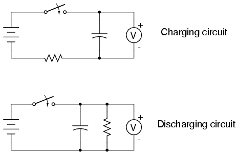
Charging and Discharging Processes
Transient Response of First-Order RC Circuits
The charging and discharging behavior of an RC circuit follows an exponential transient response governed by Kirchhoff's voltage law and the capacitor's time-dependent charge accumulation. For a series RC circuit with a DC voltage source Vs, resistor R, and capacitor C, the differential equation describing the capacitor voltage VC(t) is:
Solving this first-order linear differential equation yields the general solution for charging (initial condition VC(0) = 0):
where Ï„ = RC is the time constant. The current through the circuit during charging is:
Discharge Phase Analysis
When the voltage source is removed and the capacitor discharges through the resistor, the governing equation becomes:
With initial condition VC(0) = V0, the solution for discharging is:
The discharge current flows in the opposite direction to the charging current:
Time Constant and Practical Significance
The time constant Ï„ determines how quickly the circuit reaches equilibrium:
- At t = Ï„, the capacitor charges to ~63.2% of Vs or discharges to ~36.8% of V0
- The circuit is considered stable (~99.3% charged/discharged) after 5Ï„
In practical applications, this behavior is crucial for:
- Timing circuits in oscillators and pulse generators
- Debouncing switches in digital systems
- Analog signal filtering and coupling
Non-Ideal Considerations
Real-world RC circuits exhibit additional effects:
- Parasitic inductance affects high-frequency response
- Capacitor equivalent series resistance (ESR) modifies the effective time constant
- Dielectric absorption causes voltage rebound after discharge
The complete transient response must account for these factors in precision timing applications.
2. Differential Equation Approach
2.1 Differential Equation Approach
The behavior of an RC circuit can be rigorously analyzed using differential equations, providing a mathematical foundation for understanding transient responses. Consider a simple series RC circuit with a resistor R, capacitor C, and voltage source V(t). Applying Kirchhoff’s Voltage Law (KVL) yields:
Substituting Ohm’s Law (V_R = IR) and the capacitor’s voltage-current relationship (I = C dV_C/dt), we obtain:
This is a first-order linear ordinary differential equation (ODE) in V_C(t). For a constant input voltage V_0, the homogeneous solution describes the transient response, while the particular solution gives the steady-state behavior.
Solving the Homogeneous Equation
For the homogeneous case (V(t) = 0), the equation simplifies to:
The solution takes the form:
where τ = RC is the time constant, governing the decay rate. This exponential decay characterizes the capacitor’s discharge through the resistor.
Particular Solution and Complete Response
For a DC input V(t) = V_0, the particular solution is simply V_C = V_0. Combining homogeneous and particular solutions, the complete response for a charging capacitor is:
This equation describes the capacitor’s voltage asymptotically approaching V_0 with a time constant τ.
General Solution for Time-Varying Inputs
For arbitrary V(t), the solution is derived using an integrating factor e^{t/Ï„}:
This integral form is particularly useful for analyzing circuits with non-constant inputs, such as pulse or sinusoidal signals.
Practical Implications
The differential equation approach reveals key insights:
- Time Constant Dominance: The product RC determines the speed of transient responses.
- Filtering Behavior: High RC values attenuate high-frequency components, making RC circuits effective low-pass filters.
- Phase Shifts: In AC analysis, the capacitor introduces a frequency-dependent phase lag between voltage and current.
Step Response of RC Circuits
The step response of an RC circuit describes how the voltage across the capacitor or the current through the resistor evolves when a sudden step voltage is applied. This behavior is fundamental in signal processing, control systems, and transient analysis.
Mathematical Derivation
Consider a series RC circuit with a resistor R and capacitor C connected to a voltage source V0 via a switch. At t = 0, the switch closes, applying a step input. Kirchhoff’s Voltage Law (KVL) gives:
Since vR(t) = i(t)R and i(t) = C(dvC/dt), the differential equation becomes:
This is a first-order linear differential equation. Solving it with the initial condition vC(0) = 0 yields:
where Ï„ = RC is the time constant. The resistor voltage vR(t) follows from KVL:
Time Constant and Transient Behavior
The time constant Ï„ determines how quickly the circuit reaches steady state:
- At t = τ, the capacitor voltage reaches ≈ 63.2% of V0.
- At t = 5τ, the capacitor is considered fully charged (≈ 99.3% of V0).
The step response is characterized by an exponential rise (capacitor) or decay (resistor), critical in timing applications like pulse shaping and delay circuits.
Practical Applications
RC step response is exploited in:
- Debouncing circuits – Filtering switch transients in digital systems.
- Signal coupling – Blocking DC while passing AC signals.
- Timing circuits – Used in oscillators and monostable multivibrators.
Frequency Domain Interpretation
The step response can also be analyzed using Laplace transforms. The transfer function H(s) of the capacitor voltage is:
Inverse transforming gives the same time-domain solution, reinforcing the duality between time and frequency analysis.
Effect of Non-Ideal Components
Real-world capacitors exhibit parasitic elements like Equivalent Series Resistance (ESR) and inductance, altering the ideal step response. For high-frequency steps, these parasitics cause ringing or overshoot, necessitating careful component selection in high-speed designs.
Frequency Response and Impedance
The frequency-dependent behavior of an RC circuit is governed by the complex impedance of the capacitor, which varies with the input signal frequency. The impedance Z of a capacitor is given by:
where ω is the angular frequency (ω = 2πf) and C is the capacitance. The resistor's impedance remains constant as Z_R = R, independent of frequency.
Total Impedance of an RC Circuit
For a series RC circuit, the total impedance is the phasor sum of the resistive and capacitive impedances:
The magnitude of the impedance is:
This equation shows that at low frequencies, the capacitive reactance dominates, while at high frequencies, the resistor dominates.
Frequency Response and Cutoff Frequency
The transfer function H(ω) of a series RC circuit (voltage across the capacitor) is:
The magnitude of the transfer function is:
The cutoff frequency f_c, where the output power is halved (−3 dB point), occurs when ωRC = 1:
Below f_c, the circuit passes signals with minimal attenuation; above f_c, signals are increasingly attenuated.
Phase Shift in RC Circuits
The phase angle θ between the input and output voltages is:
At low frequencies (ω → 0), the phase shift approaches −90° (output lags input). At high frequencies (ω → ∞), the phase shift approaches 0°.
Bode Plot Representation
The frequency response is often visualized using a Bode plot, which consists of:
- Magnitude plot (dB vs. log frequency): Shows attenuation at high frequencies.
- Phase plot (degrees vs. log frequency): Illustrates the phase shift transition from −90° to 0°.
The slope of the magnitude plot is −20 dB/decade above the cutoff frequency, characteristic of a first-order low-pass filter.
Applications in Filter Design
RC circuits are fundamental in designing:
- Low-pass filters: Block high-frequency noise while passing DC and low-frequency signals.
- High-pass filters: Remove DC offsets while allowing AC signals to pass.
- Phase shifters: Used in oscillators and signal conditioning circuits.
For example, in audio systems, an RC low-pass filter can suppress high-frequency noise above the audible range, while in communication systems, high-pass RC filters remove DC bias from modulated signals.
Impedance Matching and Power Transfer
In RF circuits, the impedance of an RC network must often match the source or load impedance to maximize power transfer. The condition for maximum power transfer occurs when the load impedance is the complex conjugate of the source impedance.
For an RC circuit driving a resistive load, this requires compensating for the capacitive reactance at the operating frequency.
3. Filters: Low-Pass and High-Pass
3.1 Filters: Low-Pass and High-Pass
Fundamentals of RC Filters
An RC circuit can function as a frequency-selective filter, either attenuating high frequencies (low-pass) or low frequencies (high-pass). The behavior arises from the frequency-dependent impedance of the capacitor, given by:
At low frequencies, the capacitor's impedance dominates, while at high frequencies, the resistor's impedance becomes significant. The transition between these regimes defines the filter's cutoff frequency.
Low-Pass Filter
In a low-pass configuration, the output is taken across the capacitor. The transfer function H(ω) relates the output voltage to the input voltage:
The magnitude of the transfer function is:
The cutoff frequency fc, where the output power is halved (-3 dB point), is:
Below fc, signals pass with minimal attenuation; above fc, they are increasingly suppressed. This behavior is crucial in applications like audio signal processing and anti-aliasing in analog-to-digital converters.
High-Pass Filter
In a high-pass configuration, the output is taken across the resistor. The transfer function is:
The magnitude response is:
The cutoff frequency remains fc = 1/(2Ï€RC), but now frequencies below fc are attenuated, while higher frequencies pass through. High-pass filters are used in AC coupling and noise reduction where DC or low-frequency drift must be removed.
Phase Response
Both filters introduce a phase shift between input and output signals. For the low-pass filter, the phase angle φ is:
For the high-pass filter:
At the cutoff frequency, the phase shift is ±45°. This property is critical in feedback systems where phase margins affect stability.
Practical Considerations
Real-world implementations must account for non-ideal components. Capacitors exhibit equivalent series resistance (ESR), and resistors may have parasitic capacitance. These factors modify the actual cutoff frequency and attenuation characteristics. For precision applications, active filters using operational amplifiers are often preferred over passive RC networks.
Applications
- Low-pass: Smoothing power supply ripple, limiting bandwidth in communication systems.
- High-pass: Blocking DC offsets in audio circuits, eliminating low-frequency noise in sensor signals.
3.2 Timing Circuits and Oscillators
Basic RC Timing Circuit
The simplest form of an RC timing circuit consists of a resistor and capacitor in series, driven by a step voltage. The time constant Ï„ governs the exponential charging and discharging of the capacitor:
When a step input Vin is applied, the voltage across the capacitor VC(t) evolves as:
Conversely, during discharge, the voltage decays as:
where V0 is the initial voltage. These equations form the foundation for pulse generation and delay circuits.
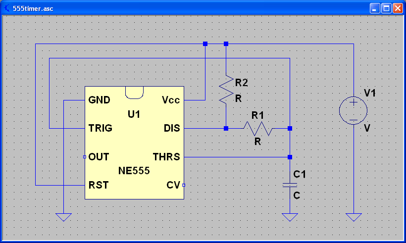
Schmitt Trigger Oscillator
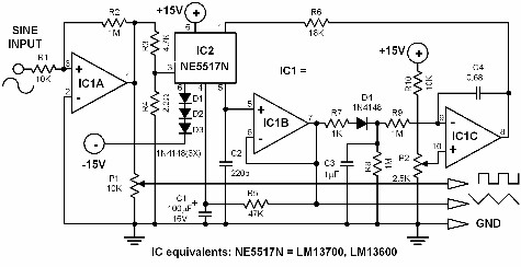
A classic RC oscillator employs a Schmitt trigger inverter to generate square waves. The hysteresis of the Schmitt trigger creates two threshold voltages, VTH (high) and VTL (low). The capacitor charges through R until it reaches VTH, triggering the output to switch low. The capacitor then discharges until it hits VTL, repeating the cycle.
The oscillation period T is derived from the charging and discharging times:
For symmetric thresholds (VTH = −VTL), this simplifies to:
Astable Multivibrator
A more precise square-wave oscillator can be built using an astable multivibrator with two transistors. The circuit alternates between two states, with each transistor's conduction period determined by an RC network. The oscillation frequency is:
This configuration is widely used in clock generation due to its simplicity and reliability.
Phase-Shift Oscillator
For sinusoidal outputs, a phase-shift oscillator employs multiple RC stages to achieve a total phase shift of 180° at the oscillation frequency. The Barkhausen criterion requires:
where β is the feedback factor and A is the amplifier gain. For a three-stage RC network, the oscillation frequency is:
and the amplifier must provide a gain of at least 29 to sustain oscillations.
Wien Bridge Oscillator
The Wien bridge oscillator offers improved frequency stability by using a balanced bridge network. The feedback loop consists of a series RC and parallel RC network, producing a phase shift of zero at the resonant frequency:
The amplifier must have a gain of exactly 3 to maintain oscillations. Automatic gain control (AGC) is often employed to stabilize the output amplitude.
Applications in Real-World Systems
- Clock Generation: RC oscillators provide low-cost timing for microcontrollers and digital systems.
- Pulse Width Modulation (PWM): Adjusting RC values modulates duty cycles in motor control and power converters.
- Signal Conditioning: Used in debounce circuits and noise filtering.
- Frequency Synthesis: Combined with PLLs, RC networks enable tunable oscillators.
3.3 Coupling and Bypass Capacitors
Coupling Capacitors
Coupling capacitors are employed in amplifier circuits to block DC components while allowing AC signals to pass. The capacitor forms a high-pass filter with the input impedance of the subsequent stage. The cutoff frequency fc is determined by:
where R is the input resistance of the next stage and C is the coupling capacitance. For minimal signal attenuation, fc should be significantly lower than the lowest frequency of interest. In audio applications, a typical value might be 10 µF for a 1 kΩ load, yielding fc ≈ 16 Hz.
Bypass Capacitors
Bypass capacitors stabilize voltage supplies by providing a low-impedance path to ground for AC signals. They are placed in parallel with emitter or source resistors in amplifier stages to prevent negative feedback from degrading AC gain. The effective impedance Zbypass is given by:
At high frequencies, the capacitor dominates, effectively shorting RE. The bypass capacitor must be large enough to maintain low impedance across the signal bandwidth. For example, a 100 µF capacitor provides ~1.6 Ω reactance at 1 kHz.
Practical Considerations
Parasitic inductance and equivalent series resistance (ESR) become critical at high frequencies. Multilayer ceramic capacitors (MLCCs) are preferred for bypass applications due to their low parasitics. For coupling, electrolytic or film capacitors are common, but their tolerance and leakage current must be accounted for in precision circuits.
Real-World Applications
- Audio Amplifiers: Coupling capacitors block DC offset between stages while bypass capacitors reduce power supply noise.
- RF Circuits: Bypass capacitors suppress high-frequency oscillations in LNA designs.
- Digital Systems: Decoupling capacitors mitigate transient current demands in IC power rails.
Mathematical Derivation: Optimal Bypass Capacitance
To derive the minimum bypass capacitance Cbypass for a given emitter resistor RE and lowest frequency fmin:
Solving for C:
For RE = 1 kΩ and fmin = 20 Hz, C ≥ 80 µF. A standard 100 µF capacitor would suffice.
4. Component Selection and Tolerance
4.1 Component Selection and Tolerance
Resistor and Capacitor Tolerance Effects
The performance of an RC circuit is critically dependent on the precision of its components. Resistors and capacitors exhibit manufacturing tolerances, typically expressed as a percentage deviation from the nominal value. For instance, a 10 kΩ resistor with ±5% tolerance may range from 9.5 kΩ to 10.5 kΩ. This variation directly impacts the time constant (τ) of the circuit:
If both components have asymmetric tolerances (e.g., R = +5%, C = -10%), the worst-case Ï„ deviates by:
For high-precision applications (e.g., filters, oscillators), 1% or 0.1% tolerance components are recommended. Military-grade or metrology circuits may require laser-trimmed resistors and NP0/C0G capacitors with ±0.05% tolerance.
Temperature and Voltage Coefficients
Beyond initial tolerance, component values drift with environmental conditions:
- Resistors: Carbon-film resistors exhibit a temperature coefficient (TCR) of ±250 ppm/°C, while metal-film types offer ±50 ppm/°C. Precision foil resistors achieve ±2 ppm/°C.
- Capacitors: Ceramic dielectrics (X7R, Y5V) show capacitance shifts up to ±15% over temperature. Polypropylene or polystyrene capacitors maintain ±1% stability.
Voltage dependence is particularly pronounced in Class II ceramic capacitors (e.g., X7R), where capacitance can drop 30% at rated voltage. This nonlinearity affects integrators and timing circuits:
where α is the voltage coefficient (typically 0.01–0.1 Vâ»Â² for BaTiO₃-based ceramics).
Parasitic Elements
Real components introduce parasitic inductance (ESL) and resistance (ESR). A multilayer ceramic capacitor (MLCC) might have 2 nH ESL and 50 mΩ ESR, forming a parasitic LC network that resonates at:
Above this frequency, the capacitor behaves inductively, degrading high-frequency bypassing. Electrolytic capacitors exhibit higher ESR (1–10 Ω), causing power dissipation (I²R losses) in high-current applications.
Statistical Analysis for Production
In mass-produced circuits, Monte Carlo analysis predicts yield by simulating component variations. For a first-order RC filter with 3σ tolerance bounds, the cutoff frequency (f_c) distribution follows:
If R and C are uncorrelated Gaussian variables, the combined standard deviation is:
This guides the selection of economically viable tolerances while meeting performance specifications. For example, a ±10% f_c tolerance might require ±5% resistors and ±2% capacitors.
Practical Selection Guidelines
- Timing circuits: Use C0G/NP0 capacitors (±30 ppm/°C) and metal-film resistors (±0.1%).
- Power supply decoupling: Prioritize low-ESR X7R ceramics (≥10 μF) paralleled with 100 nF C0G for high-frequency noise.
- High-voltage applications: Select capacitors rated ≥2× the working voltage to account for derating.
4.2 Effects of Parasitic Elements
Parasitic elements in RC circuits—such as stray capacitance, lead inductance, and equivalent series resistance (ESR)—introduce deviations from ideal behavior, particularly at high frequencies or fast switching speeds. These non-ideal components alter the circuit's transient response, frequency characteristics, and power dissipation.
Stray Capacitance
Unintentional capacitance between conductive traces, component leads, or ground planes manifests as parallel parasitic capacitance (Cp). For an RC circuit with nominal capacitance C, the effective capacitance becomes:
This shifts the circuit's time constant (Ï„ = RC) and corner frequency (f_c = 1/(2Ï€RC)). In high-frequency applications, Cp can dominate, causing unintended filtering or signal integrity issues.
Equivalent Series Resistance (ESR)
Real capacitors exhibit ESR, a parasitic resistance in series with the ideal capacitance. For a step input, the voltage across the capacitor follows:
ESR also increases power dissipation (P = I²RESR), leading to self-heating and potential thermal runaway in high-current applications.
Lead Inductance
Parasitic inductance (Lp) from component leads or PCB traces forms an unintended RLC network. The impedance becomes frequency-dependent:
At frequencies approaching the resonant point (f_r = 1/(2π√(L_pC))), the circuit exhibits peaking or ringing, compromising stability in pulse applications.
Dielectric Absorption
Imperfections in the capacitor's dielectric material cause charge retention, modeled as a parallel RC network. After discharge, a residual voltage reappears:
where kd is the dielectric absorption coefficient and Ï„d the relaxation time constant. This effect is critical in sample-and-hold circuits.
Mitigation Strategies
- Layout optimization: Minimize trace lengths and loop areas to reduce Lp and Cp.
- Component selection: Use low-ESR capacitors (e.g., ceramic) for high-frequency paths.
- Termination techniques: Series damping resistors suppress ringing caused by Lp.
4.3 Measurement Techniques
Time-Domain Analysis
Time-domain measurements of RC circuits involve analyzing the transient response to step or pulse inputs. The voltage across the capacitor VC(t) follows an exponential charging/discharging curve:
where Ï„ = RC is the time constant. An oscilloscope is typically used to capture these waveforms. Key measurements include:
- Rise time (tr): Time for the signal to transition from 10% to 90% of its final value. For an RC circuit, tr ≈ 2.2τ.
- Fall time (tf): Time for the signal to decay from 90% to 10% of its initial value.
- Time constant (Ï„): Determined by fitting the exponential curve or measuring the time to reach 63.2% of the final voltage during charging.
Frequency-Domain Analysis
Frequency response measurements reveal the circuit's behavior across different frequencies. A function generator and oscilloscope (or network analyzer) are used to measure:
The cutoff frequency (fc), where the output power is halved (-3 dB), is given by:
Phase shift measurements between input and output signals are also critical, as an RC circuit introduces a phase lag:
Impedance Spectroscopy
For advanced characterization, impedance spectroscopy measures the complex impedance Z(ω) of the RC network:
This technique is particularly useful for evaluating parasitic effects in real-world components. A frequency response analyzer (FRA) or LCR meter is employed to sweep across a wide frequency range, generating Nyquist or Bode plots.
Practical Considerations
- Probe Compensation: Oscilloscope probes must be properly compensated to avoid distorting the RC circuit's response.
- Parasitic Elements: Stray capacitance and inductance can significantly affect high-frequency measurements.
- Signal Integrity: Ensure minimal noise and proper grounding to avoid measurement artifacts.
Automated Measurement Systems
LabVIEW or Python-based automation (using libraries like PyVISA) can streamline repetitive measurements, enabling parameter sweeps (e.g., varying R or C) and real-time data logging for statistical analysis.
5. Key Textbooks and Papers
5.1 Key Textbooks and Papers
- PDF EE 233 Circuit Theory Lab 1: RC Circuits - University of Washington — EE 233 Lab 1: RC Circuits Laboratory Manual Page 2 of 11 3 Prelab Exercises 3.1 The RC Response to a DC Input 3.1.1 Charging RC Circuit The differential equation for out( ) is the most fundamental equation describing the RC circuit, and it can be solved if the input signal in( ) and an initial condition are given. Prelab #1:
- PDF ENGINEERING CIRCUIT ANALYSIS - etextbook.to — BASIC RC AND RL CIRCUITS 273 8.1 The Source-Free RC Circuit 273 8.2 Properties of the Exponential Response 277 8.3 The Source-Free RL Circuit 281 8.4 A More General Perspective 285 8.5 The Unit-Step Function 290 8.6 Driven RC Circuits 294 8.7 Driven RL Circuits 300 8.8 Predicting the Response of Sequentially Switched Circuits 303
- Lab 05 - RC Circuits.pdf - Power Supply Lab 5. RC Circuits... - Course Hero — This leakage is the repulsion of all the electrons on one side of the capacitor, and the attraction of the electron deprived opposite side. 5 V V + R Power Supply Voltmeter Capacitor Switch + Figure 5.1. Diagram of RC circuit and power supply. 33CHAPTER 5. RC CIRCUITS 34 The power supply in Figure 5.1 is represented by a battery.
- PDF Electric Circuits — and RC Circuits 220 Practical Perspective: Artificial Pacemaker 221 7.1 The Natural Response of an RL Circuit 222 7.2 The Natural Response of an RC Circuit 228 7.3 The Step Response of RL and RC Circuits 233 7.4 A General Solution for Step and Natural Responses 241 7.5 Sequential Switching 246 7.6 Unbounded Response 250
- PDF MICRCTRONIC - etextbook.to — ISBN 978--07-352960-8 (alk. paper) - ISBN -07-338045-8 (alk. paper) 1. Integrated circuits—Design and construction. 2. Semiconductors—Design and construction. 3. Electronic circuit design. I. Blalock, Travis N. II. Title. TK7874.J333 2015 621.3815—dc23 2014040020 The Internet addresses listed in the text were accurate at the time of ...
- RC Circuits - Electrical Engineering Textbooks | CircuitBread — An RC circuit is a circuit containing resistance and capacitance. As presented in Capacitance, the capacitor is an electrical component that stores electric charge, storing energy in an electric field. Figure 6.5.1(a) shows a simple . circuit that employs a dc (direct current) voltage source , a resistor , a capacitor , and a two-position switch.
- PDF RC Circuits - Michigan State University — Experiment 5 RC Circuits 5.1 Objectives • Observeandqualitativelydescribethecharginganddischarging(de-cay)ofthevoltageonacapacitor ...
- PDF Fundamentals of Electronic Circuit Design - University of Cambridge — A basic understanding of electronic circuits is important even if the designer does ... textbook. Many of the sections and figures need to be revised and/or are missing. Please check future ... 3.3 Simple RC filters 3.4 The Impedance of an Inductor 3.5 Simple RL Filters
- PDF Lecture Notes for Analog Electronics - University of Oregon — Figure 7: RC circuit | integrator. 2.0.4 A Basic RC Circuit Consider the basic RC circuit in Fig. 7. We will start by assuming that V in is a DC voltage source (e.g. a battery) and the time variation is introduced by the closing of a switch at time t = 0. We wish to solve for V out as a function of time. Applying Ohm's Law across R gives V in ...
- PDF 01 Basic Components and Electric Circuits_Final — ELECTRICAL ENGINEERING ELECTRIC CIRCUITS Comprehensive Theory with Solved Examples and Practice Questions www.madeeasypublications.org
5.2 Online Resources and Tutorials
- Circuit Analysis and Design by Ulaby and Maharbiz - University of Michigan — Chapter 5: RC and RL First-Order Circuits 5.1: Introduction to Transient Circuits 5.2: Transient Analysis and First Order Circuits 5.3: Inductors in Multisim 5.4*: Time Constants in RC Circuits Chapter 6: RLC Circuits 6.1: Piecewise Linear Sources 6.2: Exponential Sources Chapter 7: ac Analysis 7.1: Measuring Impedance with the Network Analyzer
- Basic Electronics Tutorials and Revision — Basic Electronics Tutorials and Revision Helps Beginners and Beyond Learn Basic Electronic Circuits, Engineering, and More. ... RC Charging and Discharging Circuits. 6. icon . RC Networks. ... Resistor Tutorials about resistor types and connecting them together. 13. icon . Resistors. 13Tutorials . icon . Resources. Resources Collection of ...
- PDF ECE 2120 Electrical Engineering Laboratory II - Clemson University — Lab 3 - Capacitors and Series RC Circuits 9 Lab 4 - Inductors and Series RL Circuits 18 Lab 5 - Parallel RC and RL Circuits 25 Lab 6 - Circuit Resonance 33 Lab 7 -Filters: High-pass, Low-pass, Bandpass, and Notch 42 Lab 8 - Transformers 52 Lab 9 - Two-Port Network Characterization 61 Lab 10 - Final Exam 70 Appendix A - Safety 72
- PDF EE 233 Circuit Theory Lab 1: RC Circuits - University of Washington — EE 233 Lab 1: RC Circuits Laboratory Manual Page 2 of 11 3 Prelab Exercises 3.1 The RC Response to a DC Input 3.1.1 Charging RC Circuit The differential equation for out( ) is the most fundamental equation describing the RC circuit, and it can be solved if the input signal in( ) and an initial condition are given. Prelab #1:
- PDF RC Circuits - University of Illinois Urbana-Champaign — RC Circuits • Circuits that have both resistors and capacitors: R K R Na R Cl C + + ε K ε Na ε Cl + • With resistance in the circuits capacitors do not S in the circuits, do not charge and discharge instantaneously - it takes time (even if only fractions of a second). Physics 102: Lecture 7, Slide 2 (even if only fractions of a second).
- RC Circuit - Physics Book - gatech.edu — An RC circuit can be in either series or parallel. The figure in the top right of the page shows an RC circuit. The capacitor stores electric charge (Q) RC Circuits use a DC (direct current) voltage source and the capacitor is uncharged at its initial state. In the figure below, you see an RC circuit with a switch.
- RC Circuits - Electrical Engineering Textbooks | CircuitBread — An RC circuit is a circuit containing resistance and capacitance. As presented in Capacitance, the capacitor is an electrical component that stores electric charge, storing energy in an electric field. Figure 6.5.1(a) shows a simple . circuit that employs a dc (direct current) voltage source , a resistor , a capacitor , and a two-position switch.
- PDF RC Circuits - Michigan State University — Experiment 5 RC Circuits 5.1 Objectives • Observeandqualitativelydescribethecharginganddischarging(de-cay)ofthevoltageonacapacitor ...
- PDF Lecture Notes for Analog Electronics - University of Oregon — Figure 7: RC circuit | integrator. 2.0.4 A Basic RC Circuit Consider the basic RC circuit in Fig. 7. We will start by assuming that V in is a DC voltage source (e.g. a battery) and the time variation is introduced by the closing of a switch at time t = 0. We wish to solve for V out as a function of time. Applying Ohm's Law across R gives V in ...
- 5.2: Activities - Physics LibreTexts — - Open the laptop computer file "RC_Circuits," and click the ON button in the Signal Generator window. Place the scope leads across the Output 1 signal generator outputs of the Pasco box, black to , and red to . Play around with the onscreen Waveform, Frequency and Amplitude settings (in the interest of efficiency, 2 or 3 waveforms should ...
5.3 Simulation Tools and Labs
- PDF ECE 2120 Electrical Engineering Laboratory II - Clemson University — Lab 3 - Capacitors and Series RC Circuits 9 Lab 4 - Inductors and Series RL Circuits 18 Lab 5 - Parallel RC and RL Circuits 25 Lab 6 - Circuit Resonance 33 Lab 7 -Filters: High-pass, Low-pass, Bandpass, and Notch 42 Lab 8 - Transformers 52 Lab 9 - Two-Port Network Characterization 61 Lab 10 - Final Exam 70 Appendix A - Safety 72
- PDF Laboratory Manual for AC Electrical Circuits - MVCC — 1 Introduction to RL and RC Circuits Objective In this exercise, the DC steady state response of simple RL and RC circuits is examined. The transient behavior of RC circuits is also tested. Theory Overview The DC steady state response of RL and RC circuits are essential opposite of each other: that is, once steady state is reached, capacitors behave as open circuits while inductors behave as ...
- NI myDAQ and Multisim Problems for Circuits by Ulaby and Maharbiz — m5.3 Response of the RC Circuit Figure m5.3a shows a resistor-capacitor circuit with a pair of switches and Figure m5.3a shows the switch opening-closing behavior as a function of time. The initial capacitor voltage is - 9 V. Component values are R 1 = 10 k Ω , R 2 = 3 . 3 k Ω , and R 3 = 2 . 2 k Ω , C = 1 . 0 μ F, V 1 = 9 V and V 2 = - 15 V.
- Analyzing RC and RL Circuits: Labs 5.3 & 5.4 Insights - Course Hero — LABORATORY REPORT: MODULE 4 LABS 2 Purpose The purpose of the Lab 5.3 experiment is to document and analyze the behavior of a resistor- capacitor circuit with voltage-controlled switches. This report serves to demonstrate understanding of circuit analysis principles, proficiency in using simulation software, and ability to interpret and analyze experimental data.
- 5.3: Introduction to RL and RC Circuits - Engineering LibreTexts — This page titled 5.3: Introduction to RL and RC Circuits is shared under a CC BY-NC-SA 4.0 license and was authored, remixed, and/or curated by Ramki Kalyanaraman (Cañada College) via source content that was edited to the style and standards of the LibreTexts platform.
- Lab 5 RC Circuits-new-circuit-board - Lab 5: RC Circuits ... - Studocu — The expression for current flow, while charging or discharging a capacitor, is an exponential function given by: t RC. I Im e / 5. I is the current at time t, Im is the maximum current. Equipment: RC Circuit: PASCO Charge/Discharge Circuit Board (1F capacitor, 100 resistor, battery 3, analog or digital ammeter, wires and a timer. discharge. charge
- PDF RC Circuits - Michigan State University — 5. RC Circuits VC =V0 1−e−1 ≈0.63V0 (5.4) VR =V0 e−1 ≈0.37V0 (5.5) This means that after t = τ seconds, the capacitor has been charged to63 ...
- PDF Electronic Circuit Simulation using eSim - Santhosh Thottingal — To design and implement a circuit to simulate the V-I characteristics of a diode. DESIGN AND CIRCUIT DIAGRAM Inorder to draw the diode characteristics, we have to use a DC source of voltage. Its value may be varied during simulation. The diode in the circuit should be associated with a 'diode model'. A curernt limiting resistor may
- PDF Lendi Institute of Engineering and Technology — ELECTRONIC CIRCUIT ANALYSIS LAB Lab Manual Prepared by . ECA Lab manual Dept of ECE, Lendi Institute of Engineering and Technology Page 2 LIST OF EXPERIMENTS A) TESTING IN THE HARDWARE LABORATORY:. 1. TWO STAGE RC COUPLED AMPLIFIER. 2. RC PHASE SHIFT OSCILLATOR USING TRANSISTORS. ... DESIGN AND SIMULATION USING PSPICE SOTWARE: 1. TWO STAGE RC ...
- Circuit Simulator Applet - Falstad — This is an electronic circuit simulator. When the applet starts up you will see an animated schematic of a simple LRC circuit. The green color indicates positive voltage. The gray color indicates ground. A red color indicates negative voltage. The moving yellow dots indicate current. To turn a switch on or off, just click on it.