
Relay Toggle Circuit Using a 556 Timer circuit
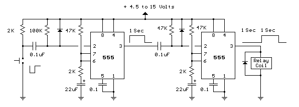
The described toggle circuit leverages the versatility of the 555 timer integrated circuit, a popular choice for various timing and oscillator applications. In this configuration, the first 555 timer is set up in an astable mode, where it continuously toggles between high and low states based on the input signals applied to pins 2 (threshold) and 6 (trigger). The output from pin 5 thus reflects the state of these inputs, functioning as an inverter.
The second 555 timer operates similarly, with its output at pin 9 inversely related to the inputs at pins 8 (trigger) and 12 (threshold). The interconnection via a 100K resistor between the output of the first timer and the input of the second timer establishes a feedback loop. This feedback ensures that when the first timer's output is high, the second timer's output is low, and vice versa.
The circuit can be utilized in various applications, such as toggling between two states in a control system, generating square wave signals, or serving as a flip-flop in digital logic circuits. The stability and reliability of the 555 timer make it an excellent choice for this type of toggle circuit, allowing for precise control over timing and signal inversion. Proper consideration should be given to the power supply and the timing capacitor values to ensure the desired frequency and performance characteristics are achieved.This toggle circuit operates by using a couple 555 timers wired as inverters. Pins 2 and 6 are the threshold and trigger inputs to the first timer and pin 5 is the output. The output at pin 5 will always be the inverse of the input at pins 2 and 6. Likewise, the output at pin 9 of the second timer will always be the inverse of the input at pins 8 and 12. A 100K resistor connects the output of one inverter to the input of the other so the state of one will be the opposite of the other..
🔗 External reference
Related Circuits
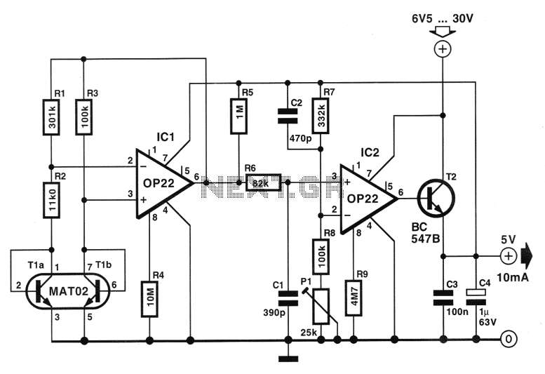
The circuit described below is notable for its low power consumption. With a 9V input and no load at the output, it draws only 50 mA, which is significantly lower than the quiescent current of a 78L05 regulator. The...
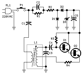
Pressing the pushbutton on the transmitter activates a sound and/or light alert in the receiver. This system operates without wiring or radio frequencies; instead, the transmitted signal is conveyed through the mains supply line. It is suitable for use...
A bandpass filter allows a specific range of frequencies to pass while rejecting frequencies that fall outside the upper and lower limits of the passband. The frequencies that are permitted to pass are referred to as the passband, which...
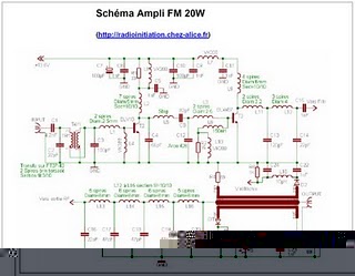
The following circuit illustrates an RF amplifier designed for FM frequencies ranging from 88 to 108 MHz with a broadband configuration. This circuit utilizes the BLV10 transistor. The RF amplifier circuit operates within the FM broadcast band, which is crucial...
This audio processor circuit utilizes the SSM2045 integrated circuit (IC), specifically designed for electronic music applications, alongside the 741 operational amplifier (op-amp) IC. The audio processor circuit is centered around the SSM2045, which is renowned for its ability to provide...
This circuit resembles an LED clock but utilizes 12 neon indicator lamps in place of LEDs. It operates on two high-capacity nickel-cadmium cells (2.5 volts), providing power for several weeks. A small switching power supply generates the high voltage...