
Sequential-timer
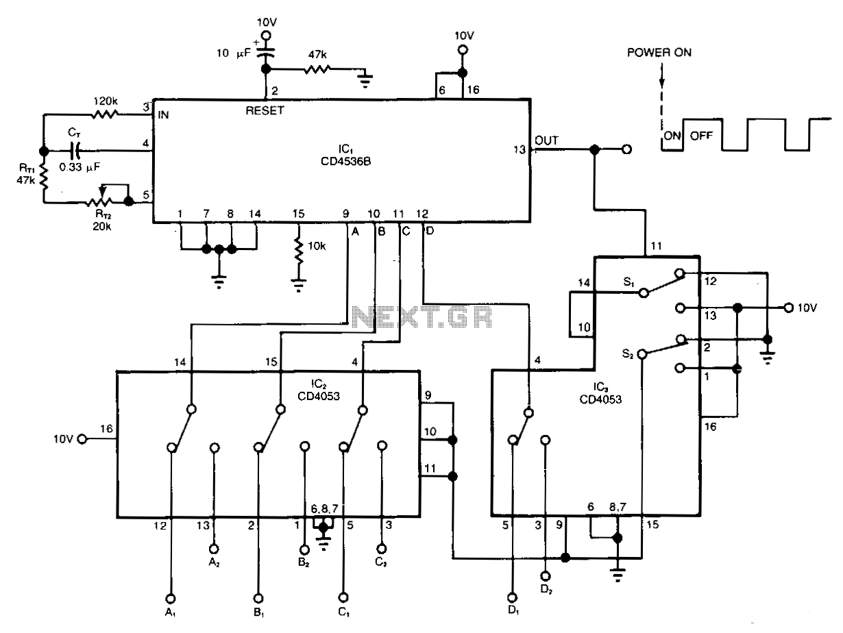
The timer circuit provides independent control over the output's on and off intervals, which can vary from 0.055 seconds to 30 minutes, and remains relatively unaffected by power-line transients. IC1 is a CMOS programmable timer chip that consists of 24 ripple-binary counter stages, with the first eight stages bypassed when a logic high is applied to pin 6. A 4-bit input code at pins A, B, C, and D connects one of the 16 remaining stages to the output at pin 13. The chip incorporates an oscillator with timing components including Cn, Rn, and R12. For this configuration, Rn is adjusted for an internal period TrN of 54.9 ms (18.2 Hz). The output on or off interval is calculated as ToUT ~ T1N 2 N-1, where N represents the number of counter stages in the internal divider chain. IC2 and IC3 are CMOS triple SPDT analog switches that connect one BCD code (A1-D1) for the on interval and another (A2-D2) for the off interval. The codes can be applied using manual toggle switches or programmable latches. Upon initial power application, the switches are positioned to apply A1-D1 to IC1, thereby generating the on interval. When the output state changes, all switches switch positions to initiate the off interval by applying A2-D2 to IC1, and this cycle continues. To prevent race conditions, switches S1 and S2 of IC3 operate sequentially before the remaining four switches operate in parallel. To initiate the output sequence with an off interval instead of an on interval, a power-on-set signal should be connected to pin 1 instead of a power-on-reset signal at pin 2.
The timer circuit described operates on the principle of programmable timing, utilizing a CMOS timer IC that incorporates both counting and timing functionalities. The core of the circuit is IC1, which allows for precise control over timing intervals through its programmable features. The 24 ripple-binary counter stages enable a wide range of timing configurations, and the ability to bypass the first eight stages provides flexibility in adjusting the timing range to accommodate various applications.
The oscillator within IC1 is critical for generating the timing pulses that determine the on and off intervals. The choice of Rn and Cn values is essential for setting the desired frequency, and the formula provided for calculating the output intervals illustrates the relationship between the selected counter stages and the timing period. This configuration allows for a high degree of customization, making it suitable for different operational requirements.
IC2 and IC3 serve as the switching mechanism that facilitates the transition between on and off states. The use of CMOS triple SPDT analog switches ensures minimal signal degradation and allows for efficient routing of the BCD codes to IC1. The design incorporates manual toggle switches or programmable latches, providing users with the option to select timing codes based on their preferences or specific applications.
The sequential operation of switches S1 and S2, followed by the parallel operation of the remaining switches, is a thoughtful design choice aimed at eliminating potential race conditions. This ensures that the timing intervals are executed reliably without unintended overlaps or timing errors. Additionally, the option to configure the circuit to start with an off interval enhances its versatility, allowing it to be tailored to specific requirements.
Overall, the timer circuit is a sophisticated and flexible solution for applications requiring precise timing control, with robust features to mitigate the effects of power-line transients and ensure reliable operation across a wide range of intervals.The timer circuit shown gives independent control of the output"s on and off intervals, which can range from 0.055 seconds to 30 minutes, relatively unaffected by power-line transients. IC1 is a CMOS programmable-timer chip that includes 24 ripple-binary counter stages; the first eight are bypassed when logic 1 is applied to pin 6.
Then, a 4-bit input code at pins A, B, C, and D connects one ofthe 16 remaining stages to the output at pin 13. The chip includes an oscillator whose timing components are Cn Rn, and R 12. For this example, you adjust R n for an internal period TrN of 54.9 ms (18.2 Hz). Then, the output on or off interval is: ToUT ~ T1N 2 N-1, where N is the number of counter stages in the internal divider chaio (See Fig. 110-3). IC2 and IC3 are CMOS triple-spdt analog switches that connect one BCD code (A I-Dl) for the on interval and another (A2-D2) for the off interval.
You can apply the codes using manual toggle switches or programmable latches. When power is first applied, the switches are in the positions shown, which applies A I -D1 to IC1 and generates the on interval. When the output changes state, all the switches change position and initiate the off interval by applying A2-D2 to IC1.
The cycle then repeats. To eliminate race conditions, switches S1 and S2 of IC3 operate in sequence before the remaining four switches operate in parallel. To start the output sequence with an off instead of an on interval, connect a power-on-set signal at pin 1 instead of the power-on-reset signal at pin 2.
🔗 External reference