
Signal-track-and-hold
When the switch is closed or the FET is conducting, the circuit functions as an inverting amplifier with a gain of R2/Rl. The inverting terminal of the op-amp acts as a virtual ground, allowing the capacitor to remain charged to the output voltage through the op-amp. When the switch is opened and the FET stops conducting, the voltage at the output is maintained by the capacitor, while the op-amp meets the current demands of the subsequent stage. The value of C should be selected so that its impedance at the operating frequency is significantly larger than that of Rl and R2.
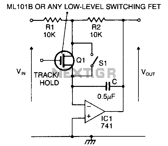
The described circuit utilizes a field-effect transistor (FET) and an operational amplifier (op-amp) to create an inverting amplifier configuration. In this setup, the FET acts as a switch that controls the flow of current through the circuit. When the switch is closed, the FET is in a conductive state, allowing the op-amp to amplify the input signal. The gain of the amplifier is determined by the ratio of the resistances R2 (feedback resistor) to Rl (input resistor), which defines the amplification factor.
The inverting terminal of the op-amp is maintained at a virtual ground level, effectively stabilizing the input signal and allowing for precise amplification. The capacitor, which is connected in the feedback loop, plays a crucial role in maintaining the output voltage. It charges to the output voltage level during the conducting state of the FET and discharges when the FET is turned off, thereby holding the output voltage constant. This behavior ensures that the output remains stable even when the switch is opened, providing a reliable voltage source for the subsequent stages of the circuit.
To optimize the performance of the circuit, the capacitance value (C) must be carefully selected. It is essential that the impedance of the capacitor at the operating frequency is much greater than the resistances Rl and R2. This condition ensures that the capacitor can effectively filter out any high-frequency noise while maintaining the desired output voltage level.
In summary, this circuit configuration exemplifies a method for achieving stable voltage output through an inverting amplifier design, leveraging the characteristics of FETs and op-amps, along with appropriate capacitor selection to ensure optimal performance in electronic applications.When the switch is closed or the FET is conducting, the circuit behaves as an inverting amplifier with a gain of R2/Rl. Since as the inverting tenninal of the op amp is a virtual ground, the capacitor is kept charged to the output voltage by the op amp.
When the switch is opened and the FET is nonconducting, the voltage at the output is held constant by the capacitor, the current demands of the next stage are met by the op amp. The value of C should be chosen so that its impedance at the operating frequency is large compared to Rl and R2. 🔗 External reference