
simple 200 watt amplifier
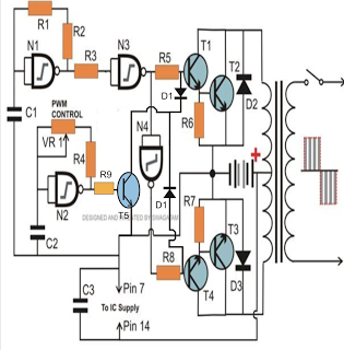
The pulses generated from the oscillator stage are square waves that serve as the basic driving pulses for the circuit. NAND gates N3 and N4 are configured as buffers to drive the output devices in tandem. While these pulses could be used to drive the inverter directly, the result would be a standard square wave inverter unsuitable for sophisticated electronic devices. Therefore, the goal is to modify the generated square waveforms to closely match a sine waveform's RMS value. This modification requires external intervention to shape the individual square waveforms.
The section comprising N2, along with associated components C2, R4, and VR1, forms another oscillator similar to N1. This oscillator produces higher-frequency, tall rectangular pulses. The output from N2 is fed into the input source of N3. Positive pulse trains from N2 are blocked by diode D1, while negative pulses are allowed through, effectively sinking relevant sections of the basic source frequency. This process creates rectangular notches in the square wave at regular intervals, determined by the frequency set by VR1. This operation cuts the basic square wave from N1 into discrete narrow sections, lowering the average RMS of the waveforms. It is recommended to use an RMS meter for proper setting adjustments.
The output devices switch the relevant transformer windings in response to these modified pulses, producing high-voltage switched waveforms at the output winding. The inverter's power can be increased from 200 watts to 500 watts, or as desired, by adding more components such as T1, T2, R5, R6, and T3, T4, R7, R8 in parallel at the appropriate points. The process of modifying square waves into sine waves can be accomplished by adjusting a single potentiometer or preset, simplifying operations. This basic concept offers high power outputs that can be optimized according to specific needs by adding additional output devices in parallel and replacing the battery and transformer with appropriately sized components.The PWM controlled modified sine wave inverter circuit presented here uses just a single 4093 for the specified functions. The IC consists of four NAND gates, out of which two are wired up as oscillators while the remaining two as buffers.
The oscillators are integrated in such a way that the high frequency from one of the oscillators interacts wi th the output of the other, generating chopped square waves whose RMS value can be well optimized to match the regular sine waveforms. Inverter designs are not always easy to understand or build, especially so when its as complex as modified sine wave types.
However the concept discussed here utilizes just a single IC 4093 for handling all the required complications. Lets learn how simple it is to build. The proposed design of a 200 watt modified sine wave inverter obtains its modified output by discretely cutting the basic square wave pulses into smaller sections of rectangular pulses.
The function resembles to a PWM control, commonly associated with IC 555. However, here the duty cycles cannot be varied separately and is kept equal throughout the available variation range. The limitation does not affect the PWM function by much, since here we are only concerned in keeping the RMS value of the output close to its sine wave counter, which is executed satisfactory through the existing configuration.
The pulses generated from this oscillator stage are square waves which forms the basic driving pulses of the circuit. N3 and N4 are wired up as buffers and are used for driving the output devices in tandem. We can easily use the above pulses solely for driving our inverter, but the result would be an ordinary square wave inverter, not suitable for operating sophisticated electronic gadgets.
Therefore, the idea is to modify the generated square waveforms so that its RMS value closely matches with a sine waveform. To do this we need to dimension the individual square waveforms through some external intervention. The section comprising N2, along with the other associated parts C2, R4 and VR1, forms another similar oscillator like N1.
However this oscillator produces higher frequencies which are tall rectangular shaped. The rectangular output from N2 is fed to the basic input source of N3. The positive trains of pulses have no effect on the source input pulses due to the presence of D1 which blocks the positive outputs from N2. However, the negative pulses are allowed by D1 and these effectively sink the relevant sections of the basic source frequency, creating kind of rectangular notches in them at regular intervals depending upon the frequency of the oscillator set by VR1.
The above operation cuts the basic square wave from N1 into discrete narrow sections, lowering the average RMS of the waveforms. It is advised that the setting is done with the help of a RMS meter. The output devices switch the relevant transformer windings in response to these dimensioned pulses and produce corresponding high voltage switched waveforms at the output winding.
The inverter power may be increased from 200 watts to 500 watts or as desired simply by adding more numbers of T1, T2, R5, R6 and T3, T4, R7, R8 in parallel over the relevant points. The modifying process of the square waves into sine waves can be done by varying a single potentiometer or rather a preset, which makes the operations pretty simple.
The concept is very basic yet offers high power outputs which may be optimized as per ones own needs just by adding a few more number of output devices in parallel and by replacing the battery and the transformer with the relevant sizes. 🔗 External reference
Related Circuits
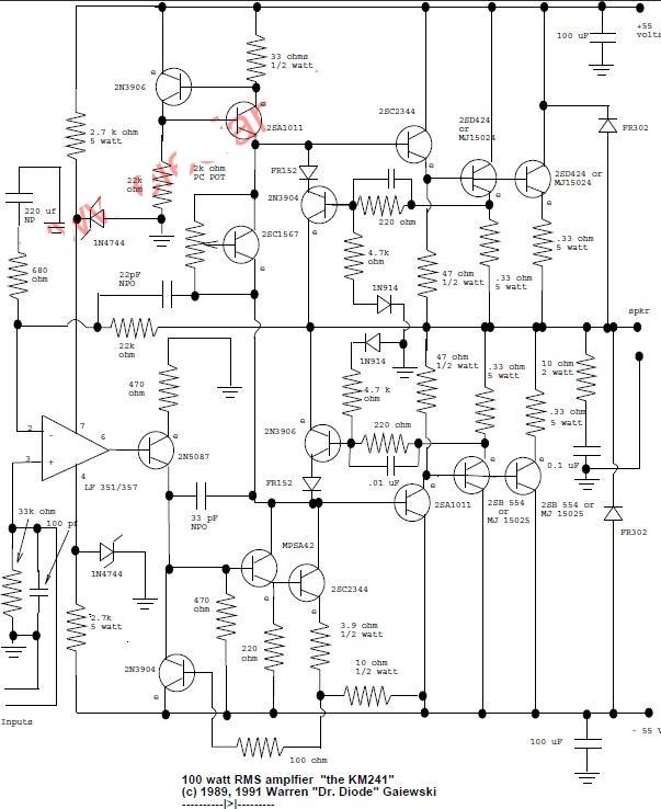
This is a 100-watt basic power amplifier designed to be relatively easy to build at a reasonable cost. It offers better performance, or musical quality, than the standard STK module amplifiers commonly found in mass-market stereo receivers. The design...
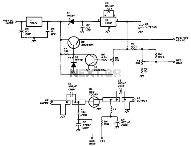
Using an NEC70083, this 1296-MHz amplifier provides approximately 17 dB of gain with a noise figure ranging from 1 to 1.5 dB. It is built on a G-10 epoxy fiberglass printed circuit board (PCB). Adhering to the specified layout...
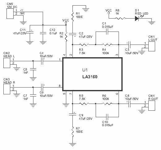
The Stereo Tape Head Preamplifier kit is based on LA3161 IC from SANYO. Power supply - 9 ~ 12 VDC @ 20 mA. Output power - upto 200 mW. Input Resistance - 100 KΩ (Typ), Load Resistance - 10...
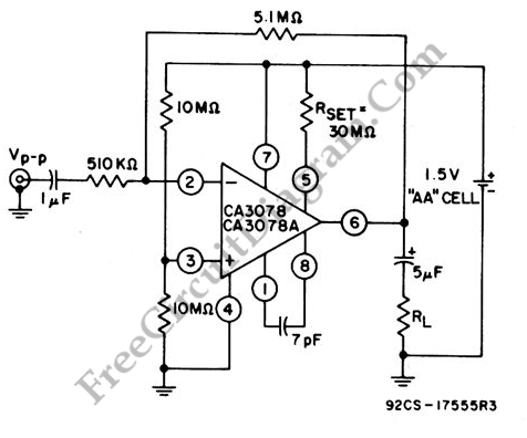
This amplifier circuit exhibits a very low power consumption, with a total current draw of 675 nA. The output voltage swing is 300 mV peak-to-peak (pp) with a gain of 20. The amplifier circuit is designed to operate with minimal...

Using an NE602 heterodyne detector and U1 as an RF amplifier, this receiver tunes the middle portion of the low-frequency spectrum from 150 to 250 kHz. U2 is a loudspeaker amplifier. The described circuit employs an NE602 integrated circuit...
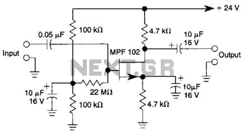
In this amplifier circuit, the gate of the MPF 102 is biased with an external voltage. This circuit achieves tighter control of the operating point and biasing conditions. The amplifier circuit utilizing the MPF 102 field-effect transistor (FET) is designed...