
sine/cosine wave oscillator
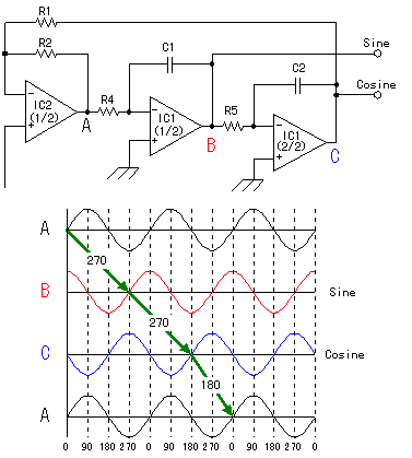
In this circuit, the operational amplifier's functionality is critical for generating oscillations based on the phase relationships between input signals and feedback. The integration circuits serve to manipulate the phase shifts necessary for stable oscillation, while the FET provides a means of dynamic feedback control to maintain desired oscillation levels. The careful design of feedback paths ensures that the oscillation remains stable and responsive to changes in input conditions, making this configuration suitable for applications requiring precise signal generation and filtering. The use of rectification to generate control voltages for the FET allows for effective modulation of the feedback loop, further enhancing the performance of the oscillator circuit.When adding an alternating current signal to the capacitor, the wave position (the phase) of the charging current of the capacitor and the voltage of the capacitor shifts by 90 degrees. When adding an alternating current signal to the coil, it changes contrary to the capacitor. The change of the voltage moves ahead by 90 degrees with the change of the current. When a signal is inputted to the positive input terminal(Noninverting input) of the operational amplifier, the operational amplifier tries to output an in-phase signal as the output. However, because there is a capacitor, the output of the operational amplifier becomes the charging current of the capacitor.
The change of the voltage of the capacitor does the change to have been 90 degrees behind with the change of the charging current. Because it is, the output signal voltage of the operational amplifier becomes the signal to be 90 degrees behind from the input signal.
When a signal is inputted to the negative input terminal(Inverting input) of the operational amplifier, the operational amplifier tries to output the signal of the antiphase( 180 ° shifted signal ) as the output. Because it is 90 degrees behind in the voltage of the capacitor from the charging current, the output voltage of the operational amplifier becomes the signal to delay 270 degrees ( 180 ° + 90 ° ) from the input signal.
At the oscillation circuit which used an amplifier circuit, oscillation operation is done when the phase of the input signal of the amplifier and the phase of the signal which is fed back from the output are in-phase. The circuit which was made this time is using the two integration circuits of the negative terminal input.
The phase difference of the input and the output of the two integration circuits shifts by the 540 degrees (180 °) and only the integration circuit doesn`t oscillate. Therefore, the loop of the oscillation is made by putting a operational amplifier (180 °) of negative terminal input.
This circuit becomes the circuit which is called "State variable-type activist filter" when it makes feed back the signal to the positive input of the IC2 from the B point. In case of the operational amplifier, the control of the gain is generally done by the feedback to the negative input.
However, this time, the negative input of the operational amplifier of the oscillation circuit is used for the oscillation operation. Therefore, it isn`t possible to do usual gain control. The circuit this time controls the oscillation voltage by the feedback of the output of IC2 to the input of IC1.
The output of IC2 is 90 degrees delayed than the negative input of IC1. When increasing the feedback from the output of IC2, the oscillation operation is suppressed. Because it is, it is possible to make do the oscillation operation which was stable if controlling the feedback in the oscillation voltage. The feedback is made both of the positive and the negative input of IC1. It is because the influence to the oscillation loop makes not become big. When there is not R3, the oscillation operation stops. I use the FET for the control of the feedback. To connect the sauce of the FET with the grounding, the feedback control is done with the positive terminal of IC1.
As for the output of the oscillator, the negative DC voltage is made with the full wave rectified. This voltage is added to the gate of the FET and the resistance value between the drain and the sauce of the FET is changed. As for the operation of the FET, refer to " Operation explanation of the sine wave oscillator ". The rectified DC voltage changes at the output voltage of the oscillator. The rectified negative voltage becomes big when the output voltage of the oscillator becomes big. Then, the resistance value between the drain and the sauce of the FET becomes big. With this, the feedback into the positive terminal of IC1 increases and the output of the oscillation decreases.
T 🔗 External reference
Related Circuits
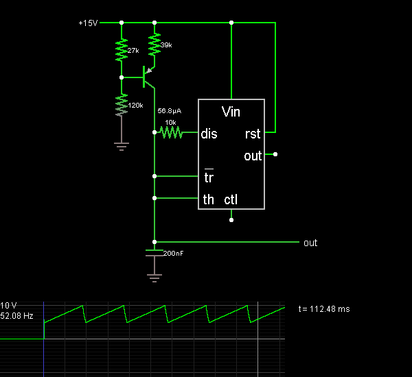
This document presents the 555 Sawtooth Oscillator circuit diagram along with a detailed explanation of its operational principles. An electronic circuit simulator is available to assist in designing the 555 Sawtooth Oscillator circuit and simulating it online for enhanced...
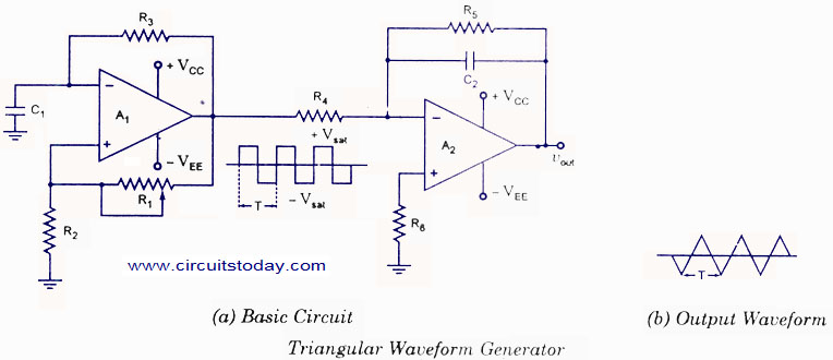
A triangular wave generator utilizing an operational amplifier (op-amp) is presented. The theoretical foundation and operation of the circuit diagram are discussed. The integration of a square wave signal results in the generation of a triangular wave. A practical...

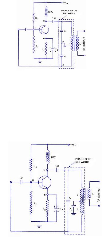
This circuit represents a negative resistance configuration. All previous circuits utilize RC time constants to achieve resonance. LC combinations can also be employed, providing good frequency stability, high Q factor, and rapid startup. In this circuit, a signal input...
This report provides details on the principles and operation of an amplifier known as the Wien Bridge Oscillator. The oscillator was designed as part of a laboratory exercise, which was not attended, thus this document will focus on the...
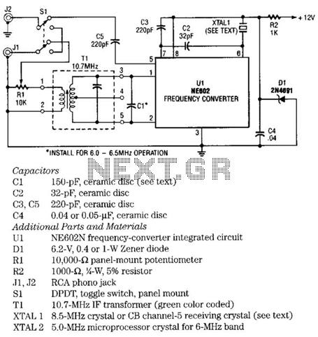
The NE602 chip, U1, contains oscillator and mixer stages. The mixer combines the oscillator signal with the input RF signal to produce signals whose frequencies are the sum and difference of the input frequencies. For example, an 8.5-MHz oscillator...
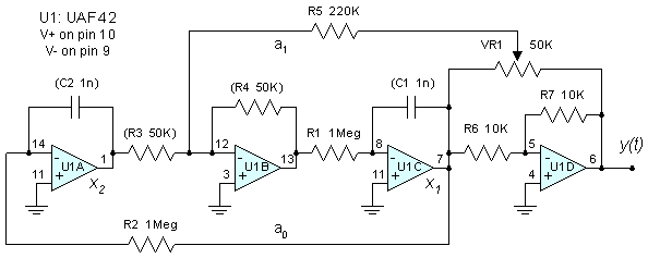
The major functional blocks necessary for designing a general-purpose audio oscillator are outlined, along with the details of the current prototype. The implementation is in the mode of an analog computer, as the desired outputs are sine and cosine...