
SINE WAVE TO SQUARE WAVE CONVERTER
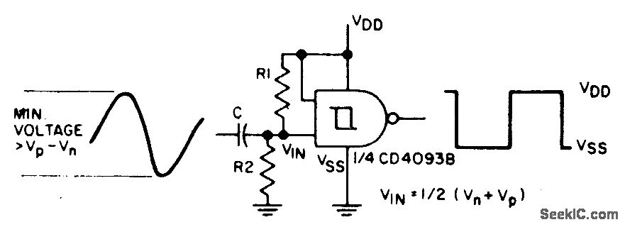
The circuit described utilizes an AC coupling technique to manage the sine input signal, which is essential for eliminating any DC offset that may affect the subsequent stages of the circuit. The capacitor C serves this purpose, allowing only the alternating current (AC) component of the signal to pass through while blocking any direct current (DC) component.
Resistors R1 and R2 are configured in a voltage divider arrangement, which establishes a bias point for the input signal. This biasing is crucial as it positions the input signal within the appropriate range between the defined threshold voltages, Vn (negative threshold) and Vp (positive threshold). By setting the bias point midway between these thresholds, the circuit ensures that the input signal can effectively toggle between high and low states, thus generating a square wave output.
The output square wave is a direct result of the input sine wave being clipped at the thresholds defined by Vn and Vp. When the input signal exceeds Vp, the output transitions to a high state, and when it falls below Vn, the output returns to a low state. This rapid transition between states creates a square wave, which is commonly used in digital circuits for clock signals or as a driving signal for other components.
Overall, the combination of AC coupling, proper biasing through R1 and R2, and the threshold management allows for effective signal processing, transforming a sinusoidal input into a square wave output suitable for further digital processing or control applications.The sine input is ac coupled by capacitor C; R1 and R2 bias the input midway between Vn and Vp, the input threshold voltages, to provide a square wave at the output. 🔗 External reference
Related Circuits

The circuit needs that the VGA card sends out the video signal in the RGB format compatible with PAL or NTSC standard video timings. This is accomplished with the right VGA to TV driver. More: This circuit is based...
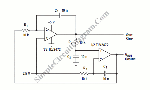
A quadrature oscillator is a type of phase shift oscillator that produces two sine wave signals, with one signal shifted by 90 degrees from the other. The quadrature oscillator is commonly used in various applications such as signal processing, communications,...
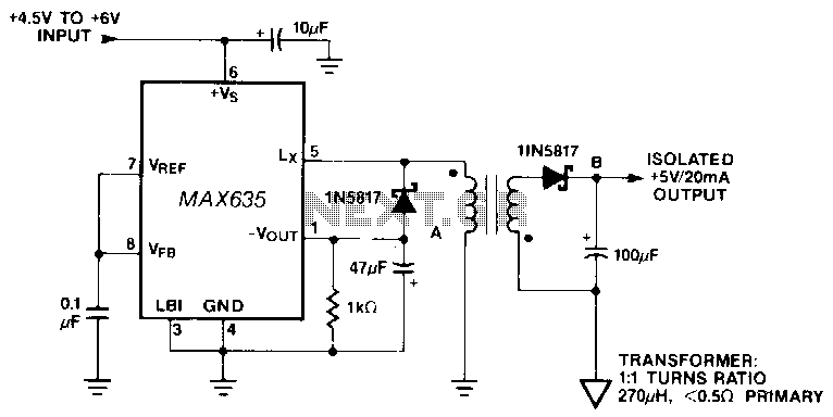
In this circuit, a negative output voltage DC-DC converter generates a -5 V output at pin A. To achieve -5 V at point A, the primary of the transformer must fly back to a diode drop that is more...
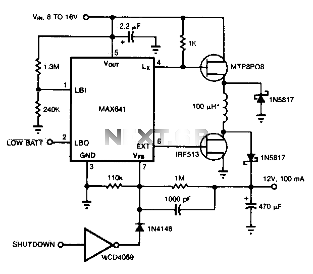
This converter can accommodate wide input voltage swings, such as the 8 to 15 V range typical of a 12 V sealed lead-acid battery. The low battery output indicates when the input voltage drops below 8 V. Pulling the...
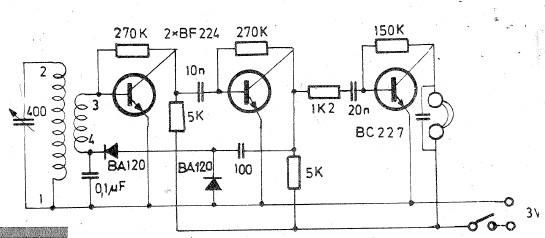
Oscillating circuits (coils) are constructed on a ferrite bar. For long wave reception, winding "1-2" consists of 135 turns, while winding "3-4" consists of 20 turns. For medium wave reception, winding "1-2" has 75 turns, and winding "3-4" has...
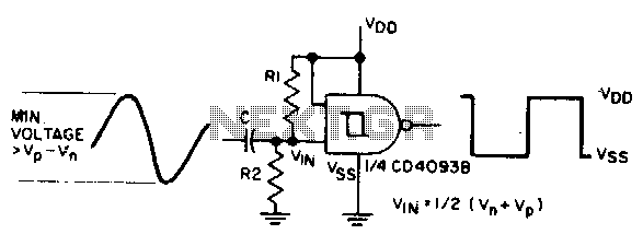
The sine input is AC coupled by capacitor C. Resistors Rl and R2 bias the input midway between Vn and Vp, which are the input threshold voltages. This configuration is designed to provide a square wave at the output. The...