
SINE WAVE TO SQUARE WAVE CONVERTER
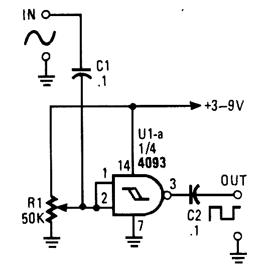
The circuit operates by utilizing the characteristics of a Schmitt trigger, which provides hysteresis in its switching behavior. This hysteresis allows the circuit to effectively handle noisy input signals, ensuring that the output remains stable and free from oscillations that could occur with a standard inverter.
In this configuration, the Schmitt trigger's two inputs are connected in such a way that one input serves as the actual signal input, while the other is used for feedback to establish the trigger levels. The trigger levels can be adjusted by modifying the resistor values in the feedback loop, allowing for flexibility in determining the precise voltage thresholds at which the output state changes.
When a sine wave is applied to the input, the voltage gradually increases and decreases, crossing the predefined trigger thresholds. As the sine wave rises and crosses the upper threshold, the output of the Schmitt trigger switches from low to high, producing a square wave that corresponds to the rising edge of the input signal. Conversely, as the sine wave descends and crosses the lower threshold, the output switches back from high to low, completing the square wave cycle.
The resulting output is a clean square wave that can be used in various applications, such as clock signals in digital circuits, waveform shaping, or as a trigger signal for other electronic components. The simplicity of this circuit, combined with the effectiveness of the Schmitt trigger in providing stable switching, makes it an ideal choice for converting analog waveforms into digital signals.This circuit tums a sine wave into a square wave. It is comprised of a single 2-input NAND Schmitt trigger that`s conftgured as an inverter with a trigger level adjustment at its input. As the input voltage rises above the gate`s trigger point, the output snaps to its alternate state, producing a square-wave output.
🔗 External reference
Related Circuits
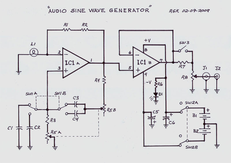
This single integrated circuit (IC) design is based on the Wien Bridge Oscillator, generating low distortion sine waves within a frequency range of 15 Hz to 22 kHz across two output voltage levels: approximately 0-250 mV and 0-2.5 Vrms....
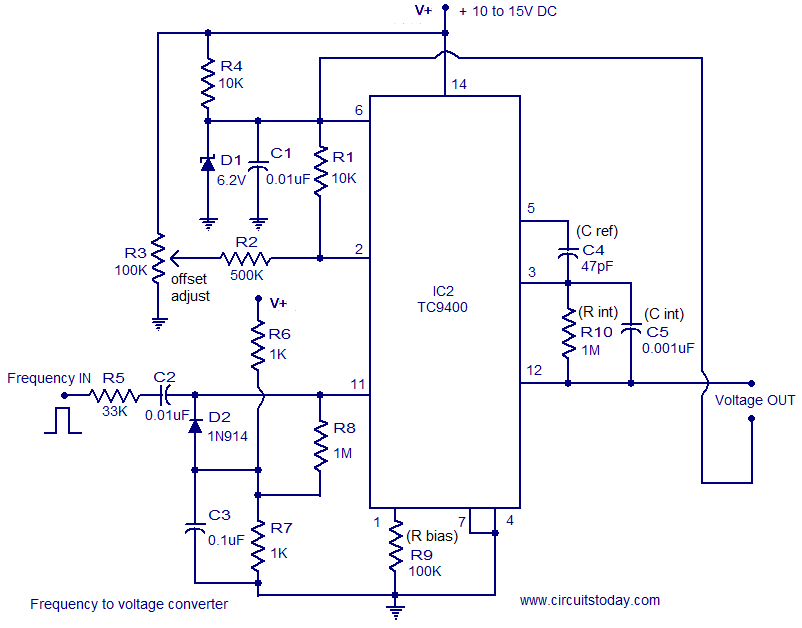
A simple and low-cost frequency-to-voltage converter based on the TC9400 IC from Microchip is presented. The TC9400 can be configured as either a voltage-to-frequency converter or a frequency-to-voltage converter, requiring minimal external components. The internal functional blocks of the...
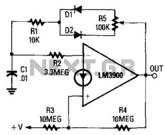
The circuit integrates a charging mechanism through Rl/Dl and the upper half of R5, while discharging occurs via R1/D2 and the lower half of R5. The duty cycle is adjustable within a range of 1:10 to 10:1 through the...
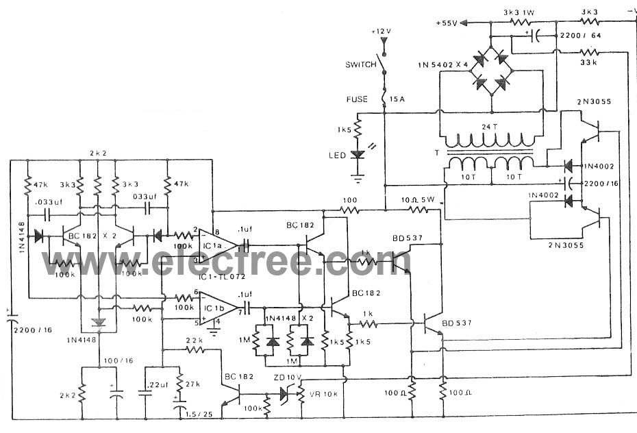
A main component along with a 2N3055 transistor and an IC TL072 is utilized in the pulse oscillator generator. The output voltage reaches +50V and -50V, providing a current of 2A to 3A. The circuit employs a 2N3055 transistor, which...
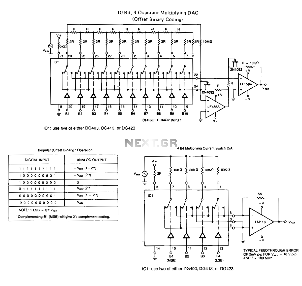
The following application circuits are intended to illustrate specific points: A 2 kΩ resistor should be placed in series with V+ to limit supply current and mitigate negative ringing of the bit inputs. Temperature compensation for Rns(on) can be...
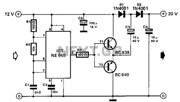
Using a 555 timer and voltage doubler, this circuit will supply over 50 mA at 20 V DC. Transistors T1 and T2 act as power amplifiers to drive the voltage doubler. The frequency of operation is approximately 8.5 kHz. The...