Solid State Relay
1. Definition and Basic Operation
Solid State Relay: Definition and Basic Operation
A solid-state relay (SSR) is an electronic switching device that operates without mechanical contacts, unlike traditional electromechanical relays. It employs semiconductor components—such as thyristors, triacs, or power transistors—to perform switching operations, enabling faster response times, higher reliability, and silent operation. SSRs are widely used in industrial automation, power electronics, and precision control systems where mechanical wear and contact arcing are undesirable.
Core Components and Functional Principle
The SSR consists of three primary subsystems:
- Input Circuit: Typically an optocoupler or low-voltage control circuit that electrically isolates the control signal from the load.
- Trigger/Driver Circuit: Converts the input signal into a form capable of activating the switching element (e.g., a zero-crossing detector for AC SSRs).
- Output Switching Element: A power semiconductor (MOSFET, TRIAC, or SCR) that handles the load current.
When a control voltage is applied to the input terminals, the optocoupler's internal LED emits infrared light, activating a photosensitive transistor or thyristor. This triggers the output semiconductor, allowing current to flow through the load. The absence of moving parts eliminates contact bounce and reduces electromagnetic interference (EMI).
Mathematical Modeling of Switching Dynamics
The turn-on time (ton) of an SSR is governed by the optocoupler's response time and the semiconductor's gate charge dynamics. For a MOSFET-based SSR, the turn-on delay can be approximated as:
where RG is the gate resistance, Ciss is the input capacitance, VDR is the driver voltage, and VTH is the threshold voltage. In AC SSRs with zero-crossing detection, the maximum turn-on delay is half the AC cycle (8.3 ms for 60 Hz systems).
Advantages Over Electromechanical Relays
- No Contact Wear: SSRs endure millions of cycles without degradation, whereas mechanical relays fail due to contact erosion.
- Silent Operation: No audible click during switching, making them ideal for noise-sensitive environments.
- High-Speed Switching: Turn-on times as low as microseconds enable precise PWM control in motor drives and heaters.
Practical Considerations
SSRs require careful thermal management due to I2R losses in the output semiconductor. The power dissipation (PD) is calculated as:
where RDS(on) is the on-state resistance (for MOSFETs) and Vf is the forward voltage drop (for TRIACs). Heat sinks or forced-air cooling are often necessary for currents exceeding 5 A.
This section provides a rigorous technical foundation for understanding SSRs, balancing theory with practical design considerations. The mathematical derivations and component-level explanations cater to advanced readers while maintaining readability through logical flow and hierarchical structuring.1.2 Comparison with Electromechanical Relays
Solid-state relays (SSRs) and electromechanical relays (EMRs) serve the same fundamental purpose of switching electrical loads, but their operational principles, performance characteristics, and application suitability differ significantly. The key distinctions arise from the absence of moving parts in SSRs, which rely on semiconductor switching elements such as thyristors, TRIACs, or MOSFETs, whereas EMRs employ physical contacts actuated by an electromagnetic coil.
Switching Speed and Lifetime
SSRs exhibit switching times in the range of microseconds to milliseconds, orders of magnitude faster than EMRs, which typically require 5–15 ms due to mechanical inertia. The absence of contact bounce in SSRs eliminates arcing, enabling reliable high-frequency switching. The lifetime of an SSR is primarily determined by semiconductor aging, often exceeding 108 cycles, whereas EMRs degrade due to contact wear, typically lasting 105–106 cycles under rated load.
Power Dissipation and Efficiency
EMRs exhibit low contact resistance (∼50 mΩ) when closed, resulting in minimal conduction losses. However, SSRs introduce forward voltage drops (1–2 V for MOSFET-based, higher for thyristors), leading to Joule heating proportional to load current:
For high-current applications, this necessitates careful thermal management. Conversely, EMRs dissipate power primarily in the actuation coil, independent of load current.
Noise and EMI Characteristics
The abrupt current interruption in EMRs generates voltage transients (L di/dt effects) and broadband electromagnetic interference. SSRs mitigate this through zero-crossing switching (for AC) or controlled slew rates in DC applications. However, high-frequency SSRs using fast semiconductors may produce higher-frequency harmonics requiring additional filtering.
Environmental Sensitivity
SSRs demonstrate superior performance in high-vibration environments and contaminated atmospheres where particulate matter could impede EMR contact movement. However, semiconductor junctions in SSRs are more susceptible to damage from voltage transients (dV/dt) and require robust snubber circuits or varistor protection. EMRs naturally withstand higher surge currents due to their physical contact geometry.
Load Compatibility
EMRs can switch both AC and DC loads indiscriminately, whereas SSRs are typically optimized for one or the other due to semiconductor physics. Specialized SSRs exist for:
- AC loads: Back-to-back thyristors or TRIACs with zero-cross detection
- DC loads: MOSFET or IGBT configurations with freewheeling diodes
Notably, SSRs excel in capacitive or inductive load switching where EMRs would suffer from contact welding during inrush currents.
Failure Modes
EMRs tend to fail open-circuit due to contact oxidation or welding, while SSRs more commonly fail short-circuit from semiconductor breakdown. This distinction critically impacts fail-safe design considerations in safety-critical systems.
1.3 Key Components and Internal Structure
Optocoupler (Input Stage)
The input stage of an SSR typically consists of an optocoupler, which electrically isolates the control circuit from the load. The optocoupler contains an infrared LED paired with a photosensitive device (e.g., photodiode, phototransistor, or phototriac). When a control voltage is applied, the LED emits light, triggering the photosensor. This galvanic isolation prevents ground loops and high-voltage transients from propagating to the low-voltage control side.
Trigger Circuit
The trigger circuit conditions the signal from the optocoupler to drive the output switching device. In AC SSRs, this often includes a zero-crossing detector to synchronize switching with the AC waveform, minimizing inrush currents. The trigger may use a Schmitt trigger or comparator to ensure clean transitions, with hysteresis to prevent chatter near threshold voltages.
Output Switching Device
The core of the SSR is its semiconductor-based output switch, which replaces the mechanical contacts of electromechanical relays. Common configurations include:
- MOSFET-based SSRs for DC loads, utilizing back-to-back N-channel or P-channel MOSFETs to block bidirectional current.
- Thyristor/Triac-based SSRs for AC loads, where antiparallel SCRs or a triac handle alternating current.
- IGBT-based SSRs for high-power applications requiring fast switching and high voltage tolerance.
Snubber Circuit
AC SSRs often incorporate an RC snubber network across the output to suppress voltage spikes caused by inductive load switching. The snubber dissipates energy during dV/dt transients, preventing false triggering or device breakdown. The time constant is designed to satisfy:
Heat Sink Interface
Power dissipation in the output switch follows:
where RDS(on) is the on-state resistance and Esw is the switching energy. A thermally conductive pad or compound ensures efficient heat transfer to an external heat sink, with thermal resistance θJA dictating maximum current ratings.
Protection Circuits
Advanced SSRs integrate:
- Transient voltage suppression (TVS) diodes to clamp overvoltages
- Current-limiting resistors for the input LED
- Status indicators (e.g., LED feedback for output state)
2. AC Output SSRs
2.1 AC Output SSRs
Operating Principle
AC output solid-state relays (SSRs) use thyristors (SCRs or TRIACs) as the switching element, enabling zero-crossing or random-phase switching of AC loads. The gate drive circuit is optically isolated, typically employing an infrared LED coupled to a photosensitive thyristor or MOSFET driver. When the input control signal activates the LED, the photodetector triggers the thyristor's gate, allowing current flow during the appropriate half-cycle of the AC waveform.
Zero-Crossing vs. Random-Phase Switching
Zero-crossing SSRs activate the thyristor only when the AC voltage crosses zero, minimizing inrush current and electromagnetic interference (EMI). This is achieved through additional zero-cross detection circuitry:
- Advantage: Reduced stress on loads and power grid
- Disadvantage: Delayed turn-on up to 8.3 ms (at 60 Hz)
Random-phase SSRs can trigger at any point in the AC cycle, enabling phase-angle control for applications like dimming or power regulation:
where α is the firing angle delay from zero-cross.
Thermal Considerations
Thyristor-based SSRs exhibit forward voltage drops (1-2 V) that generate significant heat at high currents:
Proper heatsinking is critical, with thermal resistance calculations following:
Snubber Circuits
AC SSRs require RC snubber networks (typically 100 Ω + 0.1 μF) across the thyristor to:
- Suppress dv/dt false triggering
- Limit voltage transients during turn-off
- Protect against inductive load kickback
Practical Design Constraints
Key parameters for AC SSR selection include:
- Voltage Rating: Must exceed peak line voltage (e.g., 600V device for 240VRMS AC)
- Surge Current (I2t): Critical for capacitive or motor loads
- Isolation Voltage: Typically 2.5-4 kV between control and load circuits
2.2 DC Output SSRs
DC output solid-state relays (SSRs) are designed to switch DC loads, leveraging semiconductor components such as power MOSFETs or insulated-gate bipolar transistors (IGBTs) instead of mechanical contacts. Unlike AC SSRs, which rely on zero-crossing detection for switching, DC SSRs must handle continuous current flow, requiring careful consideration of voltage drop, heat dissipation, and transient suppression.
Operating Principle
DC SSRs typically employ an optocoupler or transformer-based isolation to separate the low-voltage control circuit from the high-power DC load. The input side activates an LED or primary winding, inducing a signal in the output stage that drives the gate of a power MOSFET or IGBT. The absence of moving parts eliminates arcing, making DC SSRs ideal for high-cycle applications.
where RDS(on) is the on-state resistance of the MOSFET, Vdrop is the voltage drop across the SSR, and Iload is the load current. Minimizing RDS(on) is critical to reducing power dissipation.
Key Design Considerations
- Voltage Ratings: DC SSRs must withstand the maximum load voltage, including transients. Avalanche-rated MOSFETs are often used to handle inductive kickback.
- Current Handling: Thermal design must account for I²R losses, requiring heat sinks for high-current applications.
- Isolation: Optocouplers provide galvanic isolation, typically rated between 2.5 kV and 5 kV.
Applications
DC SSRs are widely used in:
- Battery management systems (BMS) for electric vehicles.
- Photovoltaic array switching.
- Precision DC motor control.
Transient Suppression
Inductive loads necessitate protection against voltage spikes. A freewheeling diode or transient voltage suppressor (TVS) is often placed across the load. The energy dissipated during turn-off is given by:
where L is the load inductance and I is the interrupted current.
2.3 AC/DC Input SSRs
Solid-state relays with AC or DC input control are distinguished by their input signal compatibility. The input circuit of an SSR determines its triggering mechanism, isolation method, and compatibility with different control systems. AC-input SSRs typically use a triac or back-to-back thyristors for switching, while DC-input SSRs rely on MOSFETs or IGBTs.
Input Circuit Topologies
The input stage of an SSR consists of an optocoupler or transformer-based isolation barrier, followed by a triggering circuit. For DC-input SSRs, the optocoupler's LED is driven directly by a DC voltage (typically 3–32 V). AC-input SSRs incorporate a bridge rectifier to convert the AC signal to DC before driving the optocoupler.
where VLED is the forward voltage drop of the optocoupler's LED (typically 1.2–1.5 V), ILED is the minimum required LED current (2–20 mA), and Rlim is the current-limiting resistor.
AC Input Considerations
AC-input SSRs must account for zero-crossing behavior in the control signal. The rectified input produces a pulsating DC waveform, requiring careful design of the current-limiting network to ensure reliable optocoupler operation throughout the AC cycle. The input impedance Zin is given by:
where VRMS is the RMS input voltage and IRMS is the RMS input current. Typical input impedance values range from 1 kΩ to 10 kΩ.
DC Input Characteristics
DC-input SSRs exhibit a well-defined threshold voltage, making them suitable for low-voltage control systems. The input current Iin is determined by:
where Vin is the applied DC voltage. Care must be taken to avoid exceeding the optocoupler's maximum rated current (typically 50–100 mA).
Switching Dynamics and Isolation
The isolation voltage between input and output circuits ranges from 2.5 kV to 6 kV for standard SSRs. High-voltage applications may require reinforced isolation (>10 kV). The input-to-output capacitance Cio (typically 1–10 pF) affects high-frequency noise coupling and must be minimized in sensitive applications.
Practical Design Considerations
- AC-input SSRs are preferred for direct mains-voltage control, eliminating the need for a separate DC power supply.
- DC-input SSRs offer faster response times (μs range vs. ms for AC types) and better compatibility with digital control systems.
- Input protection circuits (TVS diodes, RC snubbers) are critical for reliability in industrial environments.
Modern hybrid SSRs combine the advantages of both types, featuring universal input circuits that accept either AC or DC control signals while maintaining galvanic isolation.
Zero-Crossing and Instant-On SSRs
Solid-state relays (SSRs) are broadly classified based on their switching behavior relative to the AC waveform. The two primary modes are zero-crossing and instant-on (also called random turn-on), each optimized for distinct applications. The choice between these depends on the load characteristics, electromagnetic interference (EMI) constraints, and switching speed requirements.
Zero-Crossing SSRs
Zero-crossing SSRs activate the load only when the AC voltage waveform crosses zero volts. This is achieved using an internal zero-crossing detection circuit, typically implemented with a comparator or optocoupler synchronized to the AC cycle. The mathematical condition for triggering is:
where V(t) is the instantaneous voltage, Vpeak is the peak voltage, and f is the line frequency. The relay introduces a small delay (td) to ensure switching occurs within a narrow window around the zero-crossing point, typically ±10 ms for 50/60 Hz systems.
Advantages of zero-crossing SSRs include:
- Reduced EMI: Sudden voltage/current transitions are minimized, lowering high-frequency noise.
- Longer lifespan: Absence of inrush currents reduces stress on semiconductor components.
- Compatibility with resistive loads: Ideal for heaters, incandescent lamps, and other non-inductive devices.
However, zero-crossing SSRs are unsuitable for phase-controlled applications like dimming or motor speed control due to their inherent latency.
Instant-On SSRs
Instant-on SSRs activate the load immediately upon receiving a control signal, regardless of the AC phase. This is critical for applications requiring precise timing, such as:
- Phase-angle control for TRIAC-based dimmers.
- Rapid switching in test equipment or pulsed power systems.
- Inductive loads where zero-crossing could cause magnetic saturation.
The turn-on time (ton) for instant-on SSRs is typically under 1 ms, governed by the equation:
where Rg is the gate resistance, Ciss is the input capacitance of the switching device (e.g., MOSFET or TRIAC), Vdrive is the control voltage, and Vth is the threshold voltage.
Drawbacks include:
- Higher EMI: Abrupt switching generates harmonics and transients.
- Increased inrush currents: Capacitive or cold-filament loads may experience stress.
Practical Considerations
For inductive loads (e.g., motors, transformers), zero-crossing SSRs can cause voltage spikes due to abrupt current interruption. A snubber circuit (e.g., an RC network) is often added to mitigate this. The snubber values can be derived from:
where Ileakage is the leakage current and tfall is the fall time of the SSR.
3. Switching Mechanism
3.1 Switching Mechanism
The switching mechanism of a solid-state relay (SSR) relies on semiconductor devices rather than electromechanical contacts. Unlike traditional relays, SSRs use optocouplers, thyristors, or MOSFETs to achieve isolation and control between input and output circuits. The absence of moving parts eliminates mechanical wear, enabling faster switching speeds and higher reliability.
Optocoupler-Based Isolation
The input side of an SSR typically consists of an infrared LED, which emits light when activated by a control signal. This light is detected by a photodetector (e.g., a photodiode or phototransistor) on the output side, creating an electrically isolated trigger for the switching element. The optocoupler ensures galvanic isolation, often rated for several kilovolts.
Thyristor and Triac Switching
For AC load control, SSRs commonly employ thyristors (SCRs) or triacs. When the optocoupler triggers the gate, the thyristor enters conduction at the next zero-crossing of the AC waveform, minimizing inrush current. The turn-off occurs when the current drops below the holding threshold, typically at the next zero-crossing.
where Ihold is the holding current, Vpeak is the peak voltage, and Rload is the load resistance.
MOSFET-Based DC Switching
In DC applications, power MOSFETs are preferred due to their low on-resistance (RDS(on)) and fast switching. A back-to-back MOSFET configuration blocks current in both directions, essential for bidirectional isolation. The gate is driven by the optocoupler's output, often via an additional amplifier stage for high-current loads.
where Ploss is the conduction loss and Iload is the load current.
Zero-Crossing vs. Random Turn-On
Zero-crossing SSRs synchronize switching with the AC waveform's zero-voltage point, reducing electromagnetic interference (EMI) and inrush currents. Random-turn SSRs activate immediately upon input signal application, suitable for phase-angle control in dimming or motor speed regulation.
Thermal Considerations
Junction heating in the semiconductor switch must be managed to prevent failure. The thermal resistance (θJA) and maximum junction temperature (TJ(max)) dictate the permissible power dissipation:
where TJ is the junction temperature and TA is the ambient temperature.
3.2 Load Compatibility and Voltage Ratings
Load Types and Switching Characteristics
Solid-state relays (SSRs) exhibit distinct performance characteristics depending on the nature of the load. Resistive loads, such as heating elements, present minimal challenges due to their linear current-voltage relationship. However, inductive loads (motors, solenoids) and capacitive loads (power supplies, LED drivers) introduce transient behaviors that must be accounted for in SSR selection.
The inrush current for inductive loads can be derived from the time-domain solution of the RL circuit:
where τ = L/R is the time constant. For a motor with L = 50 mH and R = 10 Ω, the peak inrush current can reach 2-3 times the steady-state value during the first few milliseconds.
Voltage Ratings and Derating Factors
The maximum voltage rating of an SSR is determined by the blocking capability of its output semiconductor devices (typically MOSFETs or thyristors). However, three critical factors necessitate derating:
- Transient voltage spikes (L di/dt from inductive loads)
- Line voltage fluctuations (typically +10%/-15% of nominal)
- Temperature effects (blocking capability decreases at high Tj)
A practical design guideline is to select an SSR with a voltage rating of at least 2× the RMS line voltage. For 240V AC systems, this implies:
Current Handling and Thermal Considerations
The current rating of an SSR is primarily constrained by the power dissipation in the output devices. The total power loss comprises:
where Qrr is the reverse recovery charge and fsw the switching frequency. For a 40A SSR with RDS(on) = 25mΩ operating at 30A RMS:
This dissipation requires careful thermal management, as the junction-to-case thermal resistance (θJC) of typical power MOSFET packages ranges from 0.5-2°C/W.
AC vs DC Load Switching
AC-output SSRs leverage zero-crossing detection to minimize switching losses and EMI. The turn-on occurs when:
DC-output SSRs must handle continuous current without the benefit of natural zero crossings. This necessitates:
- Lower RDS(on) to reduce conduction losses
- Robust freewheeling paths for inductive loads
- Strict adherence to SOA (Safe Operating Area) curves
Surge Protection Requirements
Transient voltage suppressors (TVS diodes) must be sized according to the clamping voltage VC and peak pulse power PPP:
For a 100V surge lasting 50μs into a 50Ω load with VC = 150V:
This energy handling capability must be derated by 20-40% for high-reliability applications.
3.3 Thermal Management and Heat Dissipation
Thermal management in solid-state relays (SSRs) is critical due to power dissipation primarily occurring in the semiconductor junction. The total power loss Ploss in an SSR consists of conduction losses, switching losses (in AC SSRs), and leakage losses, given by:
where Irms is the load current, Ron the on-state resistance, Esw the switching energy, fsw the switching frequency, and Ileak the leakage current under blocking voltage Vblock.
Thermal Resistance Modeling
The junction temperature Tj must be kept below the maximum rated value (typically 125°C–150°C for silicon devices). The thermal path is modeled as a series of thermal resistances:
where:
- Ta: Ambient temperature
- θjc: Junction-to-case thermal resistance (device-specific)
- θcs: Case-to-heatsink resistance (dependent on interface material)
- θsa: Heatsink-to-ambient resistance (heatsink-dependent)
Heatsink Design Considerations
Forced air cooling or oversized heatsinks are required for high-current SSRs. The required heatsink thermal resistance is derived by rearranging the thermal equation:
For example, a 40A SSR with Ron = 5mΩ dissipating 8W at 50°C ambient with θjc = 1.2°C/W and θcs = 0.5°C/W (using thermal grease) requires:
Transient Thermal Analysis
Under pulsed loads, the thermal impedance Zth(j-a)(t) must be considered instead of steady-state θja. The Foster network model approximates this as:
where Ri and Ï„i (=RiCi) are extracted from the device datasheet.
Practical Implementation
- Interface Materials: Thermal greases (0.1–0.3°C/W), pads (0.5–2°C/W), or phase-change materials improve θcs.
- Mounting Pressure: Typically 5–15 psi for optimal contact.
- Derating Curves: SSRs exhibit reduced current capacity at high ambient temperatures, often requiring 50% derating at 70°C.
4. Industrial Automation
4.1 Industrial Automation
Role of Solid State Relays in Industrial Control Systems
Solid state relays (SSRs) are favored in industrial automation for their ability to switch high-voltage AC/DC loads with zero mechanical wear. Unlike electromechanical relays, SSRs employ semiconductor switching elements (typically thyristors, TRIACs, or MOSFETs) optically isolated from the control circuit. This eliminates contact bounce and arcing, critical in environments with explosive gases or frequent cycling.
Key Performance Metrics
The switching efficiency of an SSR in industrial applications is governed by:
where Ron is the on-state resistance (typically 10–100 mΩ for high-current SSRs) and Voff is the blocking voltage. Industrial SSRs achieve thermal stability through:
- Junction-to-case thermal resistance (θJC < 1.5°C/W for power modules)
- Active current derating above 40°C ambient temperature
Noise Immunity and Transient Protection
Industrial SSRs integrate snubber circuits to suppress dV/dt-induced false triggering. A typical RC snubber for a 480VAC system uses:
For harsh environments, SSRs incorporate:
- TVS diodes (e.g., 1.5kV clamping voltage for IEC 61000-4-5 surge protection)
- Optocouplers with 10kV/μs common-mode rejection
Real-World Implementation: Motor Control
In three-phase motor starters, SSRs enable soft-start functionality by phase-angle control. The gate drive timing for a TRIAC-based SSR is derived from:
where α is the firing angle delay. Modern industrial SSRs achieve switching times < 100μs, enabling PWM frequencies up to 1kHz for precision torque control.
Case Study: Packaging Line Automation
A high-speed bottling plant replaced electromechanical relays with optically isolated SSRs (Crydom D2425 series), resulting in:
- Cycle life improvement from 106 to >109 operations
- Reduction in maintenance downtime by 73% over 18 months
- EMI reduction meeting EN 61000-6-4 standards
Thermal Management Strategies
Industrial SSRs dissipate heat through:
- Direct mounting on DIN-rail heat sinks (thermal conductivity > 5 W/mK)
- Active cooling for currents > 50A (e.g., Fuji Electric SSR with integrated heat pipe)
The maximum junction temperature is constrained by:
where θCS is the thermal interface material resistance and θSA is the sink-to-ambient resistance.
4.2 HVAC Systems
Solid State Relay Fundamentals in HVAC Applications
Solid state relays (SSRs) provide superior performance compared to electromechanical relays in HVAC systems due to their lack of moving parts, silent operation, and faster switching speeds. The core mechanism involves optically isolated semiconductor switching elements (typically TRIACs for AC loads or MOSFETs/IGBTs for DC) that are triggered by low-voltage control signals. The absence of contact arcing enables SSRs to achieve >106 switching cycles in typical HVAC duty cycles, compared to 105 cycles for electromechanical relays.
Where thermal resistance from junction to ambient (Rth(j-a)) determines maximum current handling capacity in HVAC environments. Proper heat sinking is critical as compressor startups can produce transient currents 6-8× rated load.
Load Characteristics and Switching Considerations
HVAC systems present unique SSR challenges due to:
- Inductive kickback from compressor motors requiring snubber circuits (typically RC networks with tsnub > 10μs)
- Inrush currents demanding SSRs with 300-500% momentary overload ratings
- Zero-crossing requirements for blower motor control to minimize EMI
Advanced Protection Circuitry
Modern HVAC SSRs incorporate multiple protection layers:
Transient voltage suppressors (TVS diodes) are sized using this relation, while gate drive circuits often implement:
- dV/dt protection (typically >100V/μs rating)
- Optocoupler feedback for fault detection
- Phase-angle monitoring for soft-start algorithms
Energy Efficiency Optimization
SSRs contribute to HVAC energy efficiency through:
- Zero quiescent power in OFF state (vs. 1-3W coil consumption in EMRs)
- Precise phase-angle control enabling variable-speed compressor modulation
- Reduced I2R losses (typical ON resistance <50mΩ for 40A SSRs)
4.3 Medical Equipment
Solid-state relays (SSRs) are indispensable in modern medical devices due to their silent operation, absence of mechanical wear, and immunity to electromagnetic interference (EMI). Unlike electromechanical relays, SSRs eliminate contact bounce and arcing, critical in sensitive environments like operating rooms and diagnostic labs. Their fast switching speeds (typically <1 ms) enable precise control in applications such as defibrillators, infusion pumps, and MRI systems.
Noise-Sensitive Applications
Medical imaging systems, particularly MRI machines, demand ultra-low noise switching to prevent artifacts in acquired images. SSRs with optically isolated MOSFET or thyristor-based outputs achieve this by:
- Eliminating magnetic field interference from coil currents
- Providing galvanic isolation up to 5 kV RMS
- Maintaining leakage currents below 1 μA (IEC 60601-1 compliant)
Patient Safety Considerations
SSRs in life-support equipment must adhere to IEC 60601-1's means of patient protection (MOPP) requirements. Key design parameters include:
- Double/reinforced insulation between control and load circuits
- Creepage distances ≥8 mm for 250 VAC systems
- Overcurrent protection responding within 100 ms for fault conditions
Thermal Management in Implantable Devices
For implantable neurostimulators or pacemakers, SSRs must minimize joule heating. Power dissipation is given by:
Where RDS(on) is typically <50 mΩ for medical-grade SSRs, and Qg is kept below 10 nC through advanced packaging like wafer-level chip-scale (WLCSP) designs.
Case Study: Electrosurgical Units
In RF ablation systems operating at 300-500 kHz, SSRs replace mechanical relays for:
- Precise burst-mode control of RF energy (duty cycles from 1-100%)
- Withstanding peak voltages up to 6 kV during tissue arcing
- Maintaining CMRR >120 dB to prevent interference with monitoring ECG signals
4.4 Consumer Electronics
Solid-state relays (SSRs) are increasingly favored in consumer electronics due to their silent operation, longevity, and absence of mechanical wear. Unlike electromechanical relays, SSRs leverage semiconductor switching elements (e.g., MOSFETs, TRIACs, or thyristors) to isolate and control loads, making them ideal for noise-sensitive applications like audio equipment, smart home devices, and precision instrumentation.
Key Advantages in Consumer Applications
- Noiseless Switching: SSRs eliminate audible clicks, critical for audio systems and medical devices.
- High Reliability: With no moving parts, SSRs achieve >107 cycles, outperforming electromechanical relays by orders of magnitude.
- Compact Form Factor: PCB-mounted SSRs enable miniaturization in wearables and IoT devices.
Circuit Design Considerations
SSRs introduce unique challenges in consumer electronics, such as leakage currents and thermal management. For a TRIAC-based SSR driving a 120V AC load, the leakage current Ileak can be derived from the TRIAC's off-state impedance Zoff:
For a typical Zoff of 10 MΩ, Ileak ≈ 12 µA—sufficient to trigger false activations in high-impedance circuits. Mitigation strategies include:
- Parallel bleed resistors to shunt leakage currents
- Optocouplers with Darlington outputs for enhanced isolation
Thermal Analysis
Power dissipation Pdiss in an SSR stems from conduction losses and switching losses. For a MOSFET-based SSR with RDS(on) = 50 mΩ and Iload = 2A:
This necessitates thermal derating in compact enclosures. The junction-to-ambient thermal resistance θJA dictates the maximum allowable dissipation:
Real-World Implementations
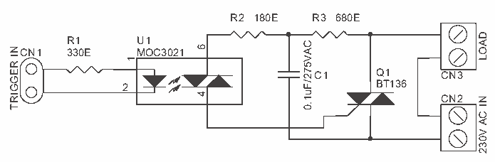
Modern smart thermostats employ SSRs for silent zone control, leveraging zero-crossing detection to minimize EMI. High-end coffee makers use SSRs for precise temperature regulation, exploiting their fast switching (<1 ms) for PID-controlled heating elements.
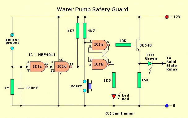
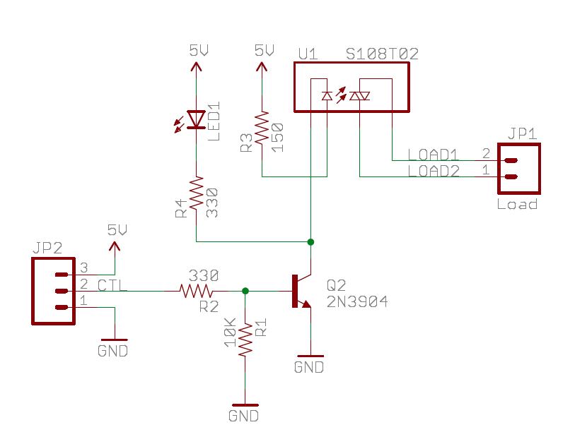
The diagram above illustrates a typical AC load control circuit, where an optocoupler isolates the low-voltage control signal from the high-voltage TRIAC stage.
5. Benefits Over Electromechanical Relays
5.1 Benefits Over Electromechanical Relays
No Moving Parts and Mechanical Wear
Solid-state relays (SSRs) eliminate mechanical contacts, relying instead on semiconductor switching elements such as thyristors, triacs, or MOSFETs. Unlike electromechanical relays (EMRs), which suffer from contact erosion due to arcing during switching, SSRs experience no wear from repeated operation. The absence of moving parts ensures a longer operational lifespan, often exceeding 108 cycles compared to 105–106 cycles for EMRs.
Faster Switching Speeds
SSRs achieve switching times in the microsecond range, whereas EMRs typically require milliseconds due to mechanical inertia. The delay in EMRs arises from the coil magnetization and physical movement of the armature. For high-frequency applications, such as pulse-width modulation (PWM) or rapid load control, SSRs provide superior performance without bounce or contact chatter.
where L and R are the coil inductance and resistance, Vcoil is the drive voltage, and Ipickup is the minimum actuation current. SSRs bypass this delay entirely.
Silent Operation and Reduced EMI
Electromechanical relays generate audible noise during contact closure and release, along with electromagnetic interference (EMI) from arcing. SSRs operate silently and produce minimal EMI since switching occurs at zero-crossing (for AC SSRs) or without abrupt current interruptions. This makes them ideal for noise-sensitive environments like medical equipment or laboratory instrumentation.
Higher Reliability in Harsh Environments
SSRs are immune to vibration, shock, and contamination—common failure modes for EMRs. Hermetically sealed optocouplers in SSRs prevent oxidation and degradation in humid or dusty conditions. Industrial applications, such as factory automation or automotive systems, benefit from this robustness.
Lower Power Consumption
EMRs require continuous coil current to maintain contact closure, dissipating power as I2R losses. SSRs only draw minimal gate-drive current, reducing steady-state power dissipation. For battery-powered or energy-efficient designs, this translates to significant savings.
where Vf is the forward voltage of the SSR's input LED.
Compact Form Factor
With no need for bulky coils or contact assemblies, SSRs occupy less board space. High-density PCBs and modular systems leverage this advantage, particularly in consumer electronics and telecom infrastructure.
5.2 Common Challenges and Mitigation Strategies
Thermal Management and Heat Dissipation
Solid state relays (SSRs) generate heat due to on-state voltage drop (VON) and switching losses. The power dissipation (PD) in an SSR is given by:
where ILOAD is the load current, RDS(ON) is the on-resistance of the MOSFET/thyristor, ESW is the switching energy, and fSW is the switching frequency. Excessive heat reduces reliability and can trigger thermal shutdown. Mitigation strategies include:
- Heat sinking: Use aluminum or copper heat sinks with thermal pads to maintain junction temperatures below 125°C.
- Forced air cooling: Employ fans for high-current (>25A) or high-frequency (>10kHz) applications.
- Derating curves: Follow manufacturer guidelines for current reduction at elevated ambient temperatures.
Voltage Transients and Surge Protection
SSRs are susceptible to voltage spikes from inductive loads (e.g., motors, solenoids). The dv/dt rating of the SSR must exceed the transient slew rate to prevent false triggering. A common mitigation approach involves:
- Snubber circuits: An RC network (e.g., 100Ω + 0.1µF) across the load suppresses high-frequency ringing.
- TVS diodes: Bidirectional transient voltage suppressors (e.g., SMAJ series) clamp spikes to safe levels.
- Varistors: Metal-oxide varistors (MOVs) with a breakdown voltage 20% above the operating voltage absorb energy from surges.
Leakage Current and Off-State Isolation
In the off state, SSRs exhibit leakage currents (typically 1–10mA) due to parasitic capacitance in the output semiconductor. This can cause:
- Ghost voltages: Misleading readings in high-impedance measurement circuits.
- Residual activation: Sensitive loads (e.g., PLC inputs) may falsely detect a closed circuit.
Solutions include:
- Bleeder resistors: A parallel resistor (e.g., 100kΩ) discharges capacitive leakage.
- Optocoupler feedback: Secondary isolation circuits verify the true off-state condition.
Zero-Crossing Artifacts in AC Switching
Zero-crossing SSRs introduce timing jitter (Δt) due to internal comparator delays, causing phase asymmetry in AC waveforms. The resulting DC offset (VDC) is:
where T is the AC period. This can saturate transformer-coupled loads. Mitigation involves:
- Precision-triggered SSRs: Use devices with <1µs synchronization error.
- DC-blocking capacitors: Series capacitors (e.g., 10µF) eliminate residual DC components.
EMI and Radio Frequency Interference (RFI)
Fast switching (especially in DC SSRs) generates broadband EMI. Radiated emissions follow:
where A is the loop area, f is the harmonic frequency, and r is the distance. Countermeasures include:
- Ferrite beads: Placed on load wires to attenuate frequencies >10MHz.
- Shielded enclosures: Conductive coatings (e.g., MuMetal) reduce far-field radiation.
- Spread-spectrum switching: Randomizing the switching frequency reduces peak emissions.
6. Key Parameters for Selection
6.1 Key Parameters for Selection
Load Voltage and Current Ratings
The load voltage (VLOAD) and current (ILOAD) ratings define the operational limits of a solid-state relay (SSR). Exceeding these values risks thermal runaway or dielectric breakdown. For AC applications, the root-mean-square (RMS) voltage must be considered, while for DC, the peak voltage must not surpass the SSR's maximum blocking voltage. The load current must account for inrush conditions, particularly in inductive or capacitive loads, where transient currents can exceed steady-state values by an order of magnitude.
where RON is the on-state resistance of the SSR. This power dissipation must be managed via heatsinking to avoid junction temperature exceedance.
Control Characteristics
The input control parameters include trigger voltage (VTRIG) and current (ITRIG), typically ranging from 3–32 VDC for voltage and 5–20 mA for current. Optically isolated SSRs often require minimal input power, while transformer-coupled variants may demand higher drive currents. The turn-on and turn-off times, typically in the microsecond to millisecond range, are critical for phase-controlled or high-frequency switching applications.
Thermal Management
The junction-to-case thermal resistance (θJC) and maximum junction temperature (TJ) dictate heatsink requirements. Forced air cooling or passive heatsinks may be necessary for high-current SSRs. The derating curve, which plots permissible load current against ambient temperature, must be consulted for reliable operation.
where TA is ambient temperature and θJA is the junction-to-ambient thermal resistance.
Isolation Voltage
The isolation voltage rating (VISO) specifies the dielectric strength between input and output, typically 2.5–6 kVRMS. This is critical for safety in high-voltage applications, such as industrial motor drives or medical equipment.
Switching Speed and Frequency
Zero-crossing SSRs minimize inrush currents in resistive loads but introduce a delay of up to half a cycle (8.3 ms at 60 Hz). Random-turn-on SSRs are preferred for phase-angle control or PWM applications. The switching frequency limit, often 1–100 Hz for electromechanical relays, can exceed 1 kHz for SSRs with fast semiconductor switches.
Protection Features
Integrated features like overvoltage protection (MOVs or snubber circuits) and overcurrent protection (e.g., I2t fusing) enhance reliability. SSRs driving inductive loads require freewheeling diodes or RC snubbers to suppress voltage transients during turn-off.
Package and Mounting
SSRs are available in PCB-mount (DIP, SMD), panel-mount, or DIN-rail configurations. The choice depends on thermal dissipation needs, creepage/clearance requirements, and mechanical constraints. Industrial-grade SSRs often feature screw terminals for high-current lugs, while compact SSRs prioritize space efficiency.
6.2 Wiring and Mounting Best Practices
Electrical Isolation and Noise Immunity
Solid-state relays (SSRs) provide galvanic isolation between control and load circuits, typically rated between 2.5 kV and 6 kV. However, improper wiring can compromise this isolation. To minimize capacitive coupling and electromagnetic interference (EMI), maintain a minimum clearance of 5 mm between high-voltage and low-voltage traces on PCBs. For chassis-mounted SSRs, use shielded cables with the shield grounded at a single point to avoid ground loops.
Where \( C_{stray} \) is the parasitic capacitance, \( \varepsilon_0 \) is the permittivity of free space, \( \varepsilon_r \) is the relative permittivity of the insulating material, \( A \) is the overlapping area of conductors, and \( d \) is the separation distance.
Thermal Management
SSRs dissipate power as heat during conduction, given by:
Where \( I_{load} \) is the load current, \( R_{on} \) is the on-state resistance, and \( V_{drop} \) is the forward voltage drop. For reliable operation, mount the SSR on a heatsink with thermal resistance \( R_{th} \) satisfying:
Here, \( T_j \) is the junction temperature, \( T_a \) is ambient temperature, and \( R_{th,j-c} \), \( R_{th,c-s} \), and \( R_{th,s-a} \) are thermal resistances from junction-to-case, case-to-sink, and sink-to-air, respectively.
Wiring Practices
- Control Signal Wiring: Use twisted-pair cables for the DC control input to reduce inductive pickup. Keep wire lengths under 3 meters for signals below 24 VDC to avoid voltage drop.
- Load Wiring: For AC loads, route phase and neutral wires parallel to minimize loop area. Use crimped lugs or screw terminals rated for the full load current.
- Surge Suppression: Snubber circuits (e.g., RC networks or MOVs) must be installed across inductive loads to suppress voltage transients exceeding the SSR's \( \frac{dV}{dt} \) rating.
Mechanical Mounting
SSRs should be mounted in an orientation that promotes convective cooling, typically with the heatsink fins vertical. Avoid mounting near heat sources or in enclosed spaces without forced airflow. For DIN rail mounting, ensure proper engagement of the rail clip and use spacers if stacking multiple relays to prevent overheating.
Torque Specifications
Terminal screws must be tightened to the manufacturer's specified torque (typically 0.5–0.6 N·m for M3 screws). Overtightening can damage the internal PCB, while undertightening increases contact resistance, leading to localized heating.
Grounding Considerations
The SSR case must be bonded to the system ground plane using a low-impedance connection. For high-frequency noise suppression, use a star grounding point and avoid daisy-chaining ground wires. The ground wire cross-section should match or exceed the load current rating.
Safety and Compliance
Verify that the SSR's insulation system meets relevant standards (e.g., UL 508, IEC 62314). Double insulation is required for medical or hazardous location applications. Always include a fast-acting fuse or circuit breaker rated at 150% of the SSR's maximum load current.
6.3 Protection Circuits and Safety Measures
Transient Voltage Suppression
Solid-state relays (SSRs) are susceptible to voltage transients, which can originate from inductive load switching, electrostatic discharge (ESD), or lightning-induced surges. A transient voltage suppressor (TVS) diode or metal-oxide varistor (MOV) is typically placed across the SSR output terminals to clamp excessive voltages. The selection criteria for a TVS diode include:
- Breakdown voltage (VBR) – Must exceed the normal operating voltage but remain below the SSR's maximum blocking voltage.
- Peak pulse current (IPP) – Determines the energy absorption capability.
- Clamping voltage (VC) – Should be low enough to protect the SSR's semiconductor junctions.
where \( R_D \) is the dynamic resistance of the TVS diode. For inductive loads, an RC snubber circuit is often added in parallel to dampen high-frequency ringing.
Overcurrent Protection
SSRs lack inherent current-limiting capability, making them vulnerable to short-circuit faults. A fast-acting fuse or electronic current limiter must be employed. The fuse's I²t rating must be lower than the SSR's surge withstand capability to ensure timely interruption. For precise protection, a crowbar circuit using a silicon-controlled rectifier (SCR) can be triggered when current exceeds a threshold:
where \( V_{gate} \) is the SCR trigger voltage and \( R_{sense} \) is a shunt resistor.
Thermal Management
Junction temperature directly impacts SSR reliability. The thermal resistance (θJA) from junction to ambient must be minimized via:
- Heat sinks – Sized based on power dissipation \( P_D = I_{load}^2 \cdot R_{on} \).
- Forced air cooling – Reduces θJA by up to 50% in high-current applications.
- Thermal cutoff switches – Disable the SSR at a preset temperature.
Zero-Crossing vs. Random Turn-On
For AC loads, zero-crossing SSRs reduce inrush current but are unsuitable for phase-controlled dimming. In such cases, a random-turn SSR with a fast-acting fuse and MOV is preferred. The trade-off between switching losses and EMI must be evaluated.
Isolation and Grounding
Optocoupler-based SSRs provide galvanic isolation, but improper grounding can compromise safety. A Faraday shield between primary and secondary circuits reduces capacitive coupling, while a ground fault interrupter (GFI) detects leakage currents exceeding 5 mA.
For high-voltage applications (>1 kV), reinforced isolation with creepage distances ≥8 mm is mandated by IEC 62368-1.
7. Recommended Books and Articles
7.1 Recommended Books and Articles
- Solid State Electronic Devices, Global Edition | Pearson eLibrary — Solid State Electronic Devices, Global Edition. 7. Auflage Erscheinungsjahr: 2015 Print-ISBN: 978-1-292-06055-2 ... One of the most widely used introductory books on semiconductor materials, physics, devices and technology, Solid State Electronic Devices aims to: 1) develop basic semiconductor physics concepts, so students can better understand ...
- PDF Solid State Electronic Devices, 7/e — with the best possible learning tools. this Global edition ... Solid State electronic devices BEn G. StrEEtMan anD Sanjay KuMar BanErjEE ... A catalogue record for this book is available from the British Library 10 9 8 7 6 5 4 3 2 1 ISBN 10:1-292-06055-7 ISBN 13: 978-1-292-06055-2
- PDF Solid-State Relay Handbook - Massachusetts Institute of Technology — a totally electronic device that depends on the electrical, magnetic, and optical properties of semiconductors and electrical components to accomplish its isolation and relay-switching functions (Fig. 1-1). The solid-state relay industry, to date, has not been noted for its standardization of relay packages.
- Solid State Electronic Devices 7th Edition - amazon.com — Solid State Electronic Devices is intended for undergraduate electrical engineering students or for practicing engineers and scientists interested in updating their understanding of modern electronics. One of the most widely used introductory books on semiconductor materials, physics, devices and technology, Solid State Electronic Devices aims to: 1) develop basic semiconductor physics ...
- Protective Relaying, 4th Edition[Book] - O'Reilly Media — 6.6 Ground Distance Relays; 6.7 Solid-State Microprocessor Relays; 6.8 Summary; Bibliography; Chapter 7 - System-Grounding Principles. 7.1 Introduction; 7.2 Ungrounded Systems; 7.3 Transient Overvoltages; 7.4 Grounded-Detection Methods for Ungrounded Systems. 7.4.1 Three-Voltage Transformers; 7.4.2 Single-Voltage Transformers; 7.5 High ...
- POWER SYSTEM RELAYING - Wiley Online Library — 2.3 Relay designs 28 2.4 Electromechanical relays 29 2.5 Solid-state relays 37 2.6 Computer relays 41 2.7 Other relay design considerations 42 2.8 Control circuits, a beginning 44 2.9 Summary 45 Problems 45 References 47 3 Current and voltage transformers 49 3.1 Introduction 49 3.2 Steady-state performance of current transformers 49
- PDF POWER SYSTEM - content.e-bookshelf.de — 2.3 Relay Designs 30 2.4 Electromechanical Relays 31 2.5 Solid-State Relays 40 2.6 Computer Relays 44 2.7 Other Relay Design Considerations 45 2.8 Control Circuits: A Beginning 48 2.9 Summary 49 Problems 49 References 51 3 Current and Voltage Transformers 53 3.1 Introduction 53 3.2 Steady-State Performance of Current Transformers 54
- PDF Solid-State Relay Reference Design User - Infineon Technologies — Solid-state relays are electronic switches capable of turning a circuit on or off using a small control signal, typically a low-voltage DC signal. Traditionally, most relays used on the market today are electromechanical, ... of use, using the connector block is recommended. 1 2 n D Figure 4 Additional connection pads . User guide 9 V 1.0 2024 ...
- (PDF) Electric Relays: Principles and Applications - ResearchGate — solid-state relays, electric thermal relays, time-delay rela ys, safety relays, and many others. On the other hand, such an artificial division within the same field frequently
- Solid State Electronic Devices Textbook - studylib.net — Textbook on solid state electronic devices, covering semiconductors, junctions, and transistors. Ideal for college-level physics and engineering students.
7.2 Technical Datasheets and Manufacturer Guides
- PDF Solid state relays Technical data - ABB — Solid-state relays Solid state relays Technical data Standard Series (R111, R115, R112) Input data R120/R121/R122R126 R311 R315 Control voltage V 4-32VDC 24-265VAC/ 24-48VDC 10-40VDC 20-265VAC/DC Make voltage, max. V 3.75VDC 22VAC/DC 10VDC 20VAC/DC Break voltage, min. V 1VDC 6VAC/DC 3VDC 5VAC/DC Input impedance kΩ 1.5 44 - - Input current max..
- Solid-State Relays Technical Documentation - Rockwell Automation — Includes: 700-SA Tube base Solid-state Relays; 700-SC Ice Cube Solid-state Relays; 700-SF Square Base Relays; 700-SH Hockey Puck Solid-state Relays; 700-SK Slim Line Solid-state Relays
- PDF Industrial relay modules and solid-state relays - Digi-Key — Weidmüller's industrial relays and solid state relays provide users with excellent reliability and service convenience. Whether electro-mechanical or electronic, our extensive choice of relay modules and solid-state relays provides the proper solution for all of your industrial application needs. Industrial relay module and solid-state relay
- Catalog Harmony Solid State Relays - English | Schneider Electric — Discover the Harmony Solid State Relays catalog from Schneider Electric. ... SSM Solid State Modular DIN Rail Relays, and SSP Solid State Panel Mount Relays. It provides technical specifications, product images, documentation, and a selection guide. The catalog aims to enhance operational efficiency and equipment availability in industrial and ...
- PDF SOLID-STATE RELAYS Opto22 Power Series SSR — to deliver a low-cost, 10-amp, solid-state relay in an all-plastic case. The push-on, tool-free quick-connect terminals make the Z Series ideal for high-volume OEM applications. Operating temperature: -40°C to 100°C. See page 7. Printed Circuit Series SSRs Opto22's Printed Circuit Series allows OEMs to easily deploy solid-state relays on
- SOLID-STATE RELAYS (SSR) - TE Connectivity — SOLID-STATE RELAYS (SSR) According to IEC 62314 for solid-state relays, the definition is "electrical relay in which the intended response is produced by electronic, magnetic, optical, or other components without mechanical motion. ... (refer to derating curves in product data sheets). An external heat sink is essential to
- PDF Solid State Relays Industrial, 1-Phase Analog Switching Type RM1E — • AC Solid State Relay • Analog switching (phase-angle control) for resistive and slightly inductive load applications • 4 - 20 mA or 0 -10 V control input • Rated operational current: 25, 50, 75, 100 and 125 AACrms • Rated operational voltage: Up to 600 VACrms • Variable intensity LED-indication according to input current
- PDF Technical Explanation for Solid-state Relays - Omron — General-purpose Relay Solid State Relay (SSR) Features Compact More compact than an SSR when the same load capacity is controlled. Enable downsizing of multi-pole relays. Etc. Enable high-speed and high-frequency switching. Unlimited number of switching operations. Consist of semiconductors, so there is no contact erosion caused by switching.
- PDF Relays with Forcibly Guided Contacts G7S- -E - Omron — Safety Relay Unit Coil Note: 1. The rated current and coil resistance are measured at a coil temperature of 23 °C with tolerances of ± 15%. 2. The maximum voltage is based on an ambient operating temperature of 23 °C maximum. Be sure to read the Safety Precautions on page 5 and the Precautions for All Relays with Forcibly Guided Contacts .
- PDF Solid-State Relays - Rockwell Automation — Manual Explanation "SSR" stands for solid-state relay. First marketed in the 1970's, SSRs have become very popular for the following reasons: • They provide a means of creating no-contact relays in output power sections enabling conversion of control circuits to ICs.
7.3 Online Resources and Tutorials
- PDF E3 and E3 Plus Solid-State Overload Relay User Manual - Rockwell Automation — †E3 Overload Relay as it applies to both the E3 and E3 Plus Overload Relays. †E3 Plus Overload Relay when features and/or functions apply specifically to it. Conventions Parameter names are shown in italic typeface. E3 refers to the overload relays E3 and E3 Plus. "E3" is the standard version. "E3 Plus" is the enhanced version.
- Protection and Switchgear | PDF | Transformer | Relay - Scribd — Online Resources To aid the faculty and ... Various case studies related to the power system are discussed as tutorials at the end ... 1.7.5 Universal Torque Equation 7 2.2.2 Definite Minimum Time Relay 36 1.8 Solid State Relay 8 2.2.3 Inverse Time Overcurrent Relay 37 1.8.1 Types of Amplitude and Phase ...
- PDF Solid-State Relay Handbook - Massachusetts Institute of Technology — a totally electronic device that depends on the electrical, magnetic, and optical properties of semiconductors and electrical components to accomplish its isolation and relay-switching functions (Fig. 1-1). The solid-state relay industry, to date, has not been noted for its standardization of relay packages.
- Solid State Electronic Devices, 7th edition - Pearson — One of the most widely used introductory books on semiconductor materials, physics, devices and technology, Solid State Electronic Devices aims to: 1) develop basic semiconductor physics concepts, so students can better understand current and future devices; and 2) provide a sound understanding of current semiconductor devices and technology ...
- PDF Understanding Solid State Switches and Their Applications — Introduced in the 1960s, the term "solid state" describes electronic devices which contain neither vacuum tubes nor mechanical devices such as relays. In solid state components, electrons flow through unheated solid semiconductor materials, Germanium or Silicon being the most well known, instead of flowing through a heated vacuum as in ...
- BLOG |HUIMU Electronics — - Why is there Silicone Gel in Solid State Relays? - As a power electronic device, solid-state relays will not use or come into contact with any liquid substances in the production process, except for silicone gel. When unpacking the plastic package of the solid-state relay, it may be found th...
- PDF GUIDE Contactors and Overload relays - ABB — 8.1 Sizing overload relays for motor applications 85 8.2 Selected Optimized Coordination (SOC) 85 9 Installations and comissioning for overload relays 87 9.1 Mounting 87 9.2 Connection 88 9.3 Motor current setting procedure 92 9.4 Overload trip test for EOL 92 9.5 Restart after tripping 93 9.6 ATEX Operating instructions 93
- PDF B1 Relay Technology - Schneider Electric Global — static relay. An example of static relay is shown in Figure B1.4. Digital protection relays introduced a step change in technology. Microprocessors and microcontrollers replaced analogue circuits used in static relays to implement relay functions. Early examples began to be introduced into service around 1980. However, such
- M3 Tutorial | PDF | Computer Program | Programming - Scribd — M3 Tutorial - Free download as PDF File (.pdf), Text File (.txt) or read online for free. This document provides an overview of programming a Millenium 3 logic controller. It describes the two available programming languages - Ladder Logic (LD) and Function Block Diagrams (FBD). FBD is recommended for more complex applications as it allows for analog inputs, arithmetic operations, and uses ...