
Spike Detector For Oscilloscopes
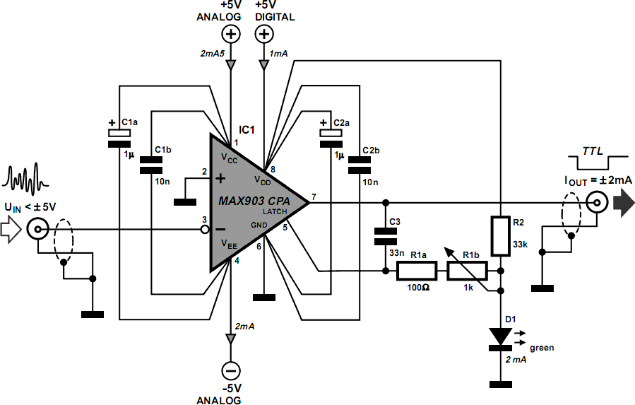
The MAX903 comparator is critical for applications requiring high-speed pulse detection and processing. It is capable of responding to very short input signals, making it suitable for precise timing applications such as laser pulse detection. The internal latch mechanism plays a significant role in pulse manipulation, allowing for the extension of short pulses which can be beneficial in systems where pulse width modulation is necessary. The design emphasizes the importance of careful PCB layout to minimize noise and ensure signal integrity, which is essential for maintaining the performance of high-speed electronics. The use of separate power supplies for the analog and digital sections helps to further isolate the sensitive components from noise, enhancing the reliability of the circuit. Proper grounding techniques, such as soldering the coax cable directly to the ground plane, are also crucial for reducing electromagnetic interference and ensuring stable operation. The flexibility of the circuit design allows for adaptation to various input conditions, making it a versatile choice for engineers working with high-speed signal processing applications.Dynamic‚ip-‚ops ignore pulses at their inputs that are shorter than 40 ns or do not have TTL levels. This means that TTL flip-flops are poorly suited to capturing noise pulses having unknown durations and magnitudes. Anyone who has ever tried to observe very short laser pulses (15 25 ns) is familiar with this problem.
By contrast, this circ uit can detect impulses with widths less than 8 ns and amplitudes between +100 mV and +5 V. The heart of this circuit is formed by a MAX903, a very fast comparator with internal memory. The IC has separate supply pins for its analogue and digital portions. The analogue portion is powered by a symmetrical ±5-V supply. This allows the detector to also handle input voltages that are negative relative to ground. The internal memory and output stage operate from a single-ended +5-V supply, so the output signal has proper TTL levels. The MAX903 (IC1) has a special internal memory circuit (latch). The latch either connects the output of the internal comparator directly to the signal output or stores the most recent TTL level and blocks the output of the internal comparator, causing the most recent TTL level appears at the output.
This allows short input pulses to be stretched to any desired length. Despite its extremely short switching times, the MAX903 consumes only a modest 18 mW. In the quiescent state, the voltage on the Latch input (pin 5) is at 1. 75 V. This reference voltage is provided by LED D1, which draws its current via R2. In this state the latch is transparent, and a positive edge at the input appears will appear as a negative transition on the output after a propagation delay of 8 ns (tPD). This only happens if the peak voltage on the input is more positive than ground potential. C1 passes this change in the output voltage level to the Latch input (pin 5). As soon as the voltage on the Latch input drops below 1. 4 V, the internal latch switches to the Hold state. In this state, the output is no longer connected to the comparator, and the output remains low for the duration of the latch hold time, regardless of what happens with the input signal.
The latch hold time is determined by the time constant of the C3/R1 network; it has an adjustment range of 100 500 ns. Pulses of this length can be readily observed using practically any oscilloscope. This latch function in this circuit is only triggered if the input signal has a rising edge that crosses the zero-voltage level.
The internal latch remains transparent for signals in the range of 5 V to 0 V, so such pulses will not be stretched. If only positive input voltages are anticipated, the negative supply voltage is not necessary and the circuit can be powered from a single +5-V supply.
A fast circuit such as this requires a carefully designed circuit board layout. All connections to the IC must be kept very short. Decoupling capacitors C1 and C2 should preferably be placed immediately adjacent to the supply pins. Pin 3 of the IC can be bent upward and soldered directly to a length of coax or twisted-pair cable (air is still the best insulator). If a coax cable is used, the unbraided screen must not be formed into a long pigtail. It`s better to peel back a short length of the screen, wrap a length of bare wire around it and solder it directly to the ground plane.
The supply traces for the analogue and digital portions must be well separated from each other, and each supply must be well decoupled, even if only a single supply voltage (+5 V) is used. The preferred solution is to use two independent voltage regulators. 🔗 External reference
Related Circuits
A simple proximity detector can be created using this electronic circuit. This circuit responds to the presence of a conductive object within a specific range. The sensitivity of the circuit can be adjusted with potentiometer P1 to achieve the...
A single chip metal detector with a range of a few inches. This is useful for detecting nails or screws in walls and floors, or for locating buried mains cable. The heart of the circuit is a single IC,...

An arrangement was established that functions effectively. In the siren circuit, the reed switch was shorted as illustrated. The power supply was removed, and a new configuration was created. The described siren circuit utilizes a reed switch, which is a...
The hardware for this project had three main components: laser gun assembly, detector unit, control pad. The detector unit's function was to simply detect a laser pulse over a small area sent by the laser driver circuit on the...
One of the simplest methods to demonstrate the autonomous motion of a robot is by having it follow a line. There are competitions for the fastest robots or those capable of navigating complex line mazes. Lines can be high-contrast...
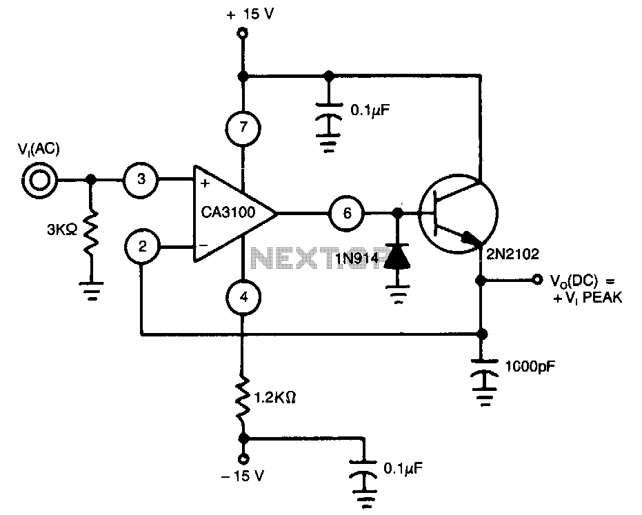
This peak detector utilizes a CA3100 BiMOS operational amplifier configured as a wide-band non-inverting amplifier, ensuring a nearly constant gain across a broad spectrum of input frequencies. The IN914 diode clips the negative half of the voltage defined by...