
STA550 - 2 x 70W Audio Amplifier Circuit
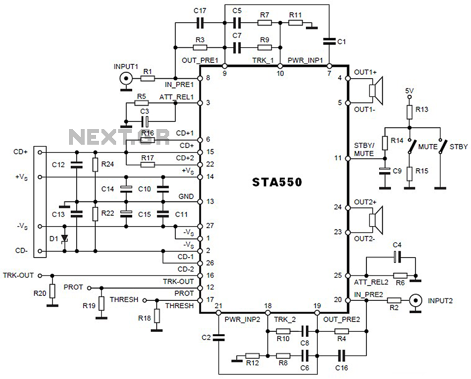
The 2 x 70W audio power amplifier circuit utilizing the STA550 IC is designed to deliver robust audio performance with a dual-channel output. The circuit's simplicity is attributed to its reliance on a minimal number of external components, which primarily include resistors and capacitors that shape the amplifier's frequency response and gain characteristics. The STA550 is engineered for high efficiency, allowing it to achieve substantial output power while managing thermal performance effectively.
The power supply requirements are critical for the correct operation of the amplifier. The dual voltage supply ensures that the amplifier can handle a wide dynamic range and provides the necessary headroom for audio signals. The specified voltage ranges for +Vs and -Vs are designed to optimize performance while preventing distortion or clipping during operation. The tracking rails, VCD+ and VCD-, are essential for maintaining the stability of the amplifier under varying load conditions.
The gain configuration, determined by the resistor ratios R1/R3 and R2/R4, allows for versatility in audio applications. This feature is particularly beneficial in scenarios where the input signal level may be insufficient. By adjusting the resistor values, the designer can tailor the gain to suit specific input conditions without compromising the integrity of the audio signal. The operating current limit, defined by Iin_max, ensures that the amplifier remains within safe operating conditions, thereby enhancing reliability and longevity.
This amplifier circuit is suitable for a variety of applications, including home audio systems, public address systems, and musical instrument amplification, where high fidelity and power output are essential. The design principles employed in the STA550 amplifier circuit exemplify modern approaches to audio amplification, combining efficiency, simplicity, and flexibility.This is a 2 x 70W audio power amplifier circuit which built using single IC STA550. The amplifier circuit require few external components (most of them are resistors and capacitors) and is very easy to design The STA550 audio amplifier is capable to provide a maximum output power of 70 watts on two channels (70 + 70 watts). This power amplifier ci rcuit require a multi voltage power supply, because the amplifier require : +Vs Positive supply voltage referred to pin 13 (GND), Negative supply voltage referred to pin 13 (GND) -Vs, VCD+ Positive supply voltage tracking rail, VCD- Negative supply voltage tracking rail. The +Vs Positive supply voltage can be : +20 to +30 volts, -Vs Negative supply voltage : -10 to -22 volts, Positive supply voltage tracking rail VCD+ : +3 to 17 volts, Negative supply voltage tracking rail VCD- : -17 to -3 volts.
VCD- must not be more negative than -Vs and VCD+ must not be more positive than +VS. In this circuit diagram, R1/R3 (or R2/R4) ratio fix the gain of the preamplifier. If the input signal is very low, is possible to increase the gain fixing the product Vin*G = cost. In that case is possible to increase G decreasing R1, 2 from 10KW until 2KW without relevant effetcs on the circuit behavior and remaining in the operating range Iin_max = Vin_max/R1(2) <1ma. >This is a 2 x 70W audio power amplifier circuit which built using single IC STA550. 🔗 External reference
Related Circuits
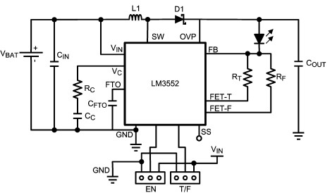
For this LED driver electronic project, a DC power supply circuit is required to provide an output voltage between 2.7V and 5.5V. The supply voltage must be applied between Vin and GND. The T/F jumper connects the T post...

A simple FM transmitter circuit can be designed using the MC2833 integrated circuit, which is intended for cordless telephone and FM communication applications. This circuit includes a microphone amplifier, a voltage-controlled oscillator, and two auxiliary transistors. The final output...
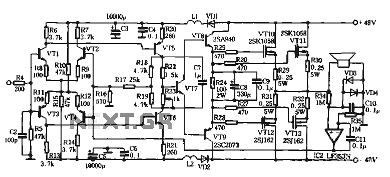
The self-designed amplifier circuit described is completely symmetrical and complementary, effectively utilizing the advantages of complementary NPN and PNP transistors to achieve a high degree of stability. The circuit features good symmetry in the push-pull amplification state, allowing for...
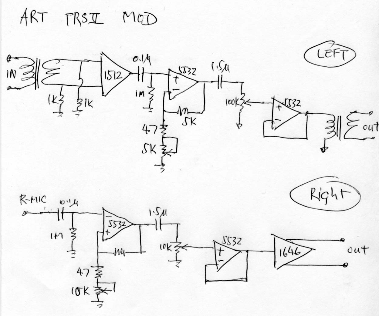
The ART TPS2 is a starved tube microphone preamplifier that utilizes a single 12AX7 tube operating at approximately 50V plate voltage to enhance the sound quality. Initially, the intention was to construct an entirely solid-state preamp, leading to the...

This display driver circuit illustrates how a Seven Segment Display is driven using the 5-stage Johnson decade counter IC CD4033. The integrated circuit functions as a counter. The CD4033 is a versatile decade counter that can be utilized to drive...
The circuit operates using an integrated circuit (IC) NE555 along with resistors R, RP, and capacitor C3, forming an astable multivibrator configuration. The output from pin 3 of the IC generates a square wave oscillation signal, which is passed...