Stabilized-capacitance-buffer

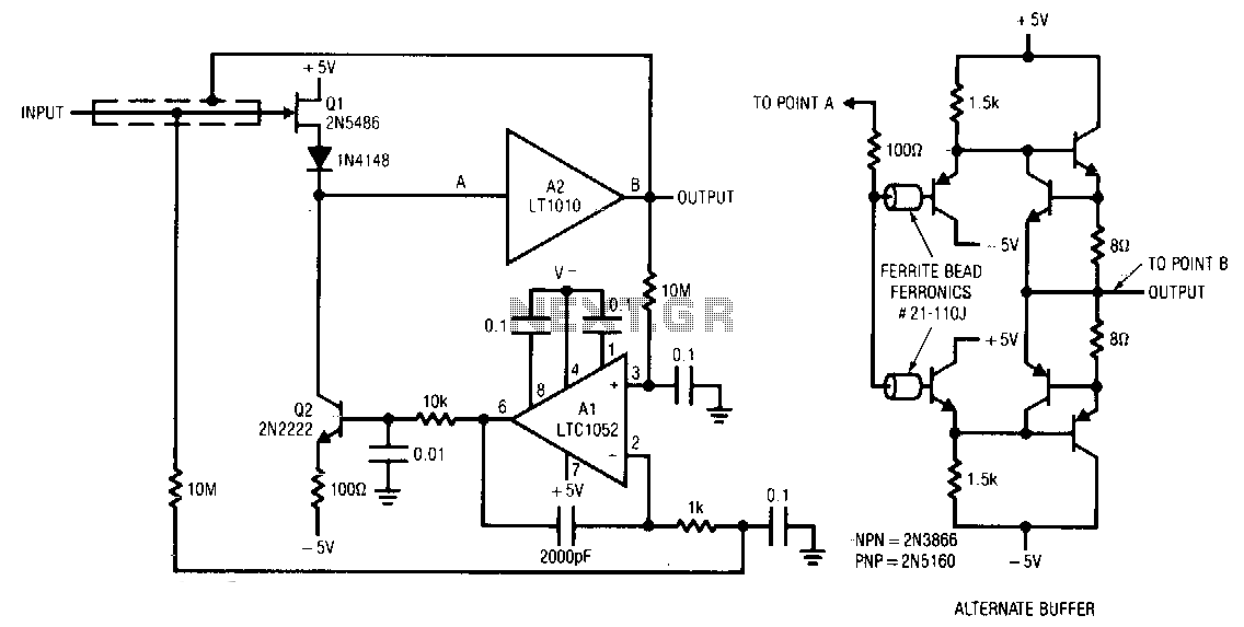
Q1 and Q2 form a simple, high-speed FET input buffer. Q1 operates as a source follower, while Q2 serves as a current source load that sets the drain-source channel current. The LT1010 buffer provides the necessary output drive capability for cables or any required load. Typically, this open-loop configuration would exhibit significant drift due to the absence of negative feedback. The LTC1052 introduces this feedback function to stabilize the circuit by comparing the filtered output of the circuit to a similarly filtered version of the input signal. The amplified difference between these signals is utilized to adjust Q2's bias, thereby controlling Q1's channel current. Q1's source line ensures that the gate never becomes forward biased, and the 2000 pF capacitor at A1 offers stable loop compensation. The RC network at A1's output prevents the circuit from encountering high-speed edges that may couple through Q2's collector-base junction. Additionally, A2's output is fed back to the shield surrounding Q1's gate lead, effectively bootstrapping the circuit's input capacitance down to less than 1 pF.
The circuit described utilizes Q1 and Q2 as integral components of a high-speed FET input buffer, designed to maintain signal integrity while minimizing drift. Q1, configured as a source follower, allows for a high input impedance and low output impedance, making it ideal for interfacing with various loads. The current source provided by Q2 stabilizes the drain-source channel current, ensuring consistent performance across varying operational conditions.
The LT1010 buffer is crucial for driving output loads, enabling the circuit to handle signal transmission over cables or other connections without distortion. The absence of negative feedback in a typical open-loop configuration could lead to instability; however, the LTC1052 mitigates this issue by introducing feedback that compares the output signal to the input signal. This feedback mechanism adjusts Q2's bias based on the amplified difference between the two signals, thereby modulating Q1's channel current to maintain stability.
The inclusion of a 2000 pF capacitor at A1 is vital for loop compensation, ensuring that the feedback loop remains stable under dynamic conditions. The RC network at A1's output serves to filter out high-frequency noise that could otherwise couple through Q2's collector-base junction, preserving the signal's integrity. Furthermore, the feedback from A2's output to the shield around Q1's gate lead effectively reduces the input capacitance to less than 1 pF, enhancing the circuit's performance in high-speed applications.
Overall, this circuit design demonstrates a sophisticated approach to buffering and signal conditioning, leveraging feedback and compensation techniques to achieve high-speed operation with minimal distortion and drift.Ql and Q2 constitute a simple, high-speed FET input buffer. Ql functions as a source follower, with the Q2 current source load setting the drain-source channel current. The LT1010 buffer provides output drive capability for cables or whatever load is required. Normally, this open-loop configuration would be quite drifty because there is no de feedback. The LTC1052 contributes this function to stabilize the circuit. It does this by comparing the filtered circuit output to a similarly filtered version of the input signal.
The amplified difference between these signals is used to set Q2"s bias, and hence Ql "s channel current. Ql "s source line ensures that the gate never forward biases, and the 2000 pF capacitor at Al provides stable loop compensation.
The rc network in Al"s output prevents it from seeing high-speed edges coupled through Q2"s collector-base junction. A2"s output is also fed back to the shield around Ql"s gate lead, bootstrapping the circuit"s effective in_put capacitance down to less than 1 pF.