
Switchable Output Crystal Oscillator
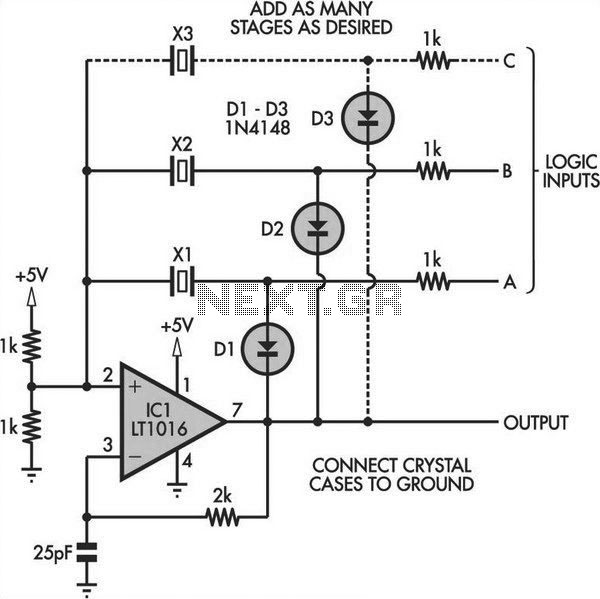
The switchable output crystal oscillator circuit is designed to provide precise frequency generation by utilizing multiple crystal resonators that can be selected via digital logic signals. The fundamental operation of this circuit involves the integration of a microcontroller or a logic gate array that interfaces with a set of crystal oscillators. Each crystal oscillator is tuned to a specific frequency, and the selection mechanism relies on electronic switching, typically achieved through analog switches or multiplexers.
In the circuit, the microcontroller sends control signals to the switching mechanism, enabling the desired crystal oscillator while disabling the others. This allows for dynamic frequency adjustment without the need for mechanical switching, which can introduce wear and reliability issues. The output of the selected crystal oscillator is then fed into a buffer stage to ensure signal integrity and drive capability, allowing the output to interface with other circuit components or systems.
The circuit design should include considerations for power supply decoupling, ensuring stable operation of the oscillators. Additionally, the layout should minimize parasitic capacitance and inductance, which can adversely affect the frequency stability and performance of the oscillators. Proper grounding techniques and the use of ground planes can further enhance the circuit's performance.
Overall, this switchable output crystal oscillator circuit is highly versatile and can be employed in various applications such as communication systems, signal processing, and frequency synthesis, where precise timing and frequency control are essential.Switchable Output Crystal Oscillator Circuit This oscillator circuit permits crystals to be electronically switched by logic commands. The circuit is best understood by initially ignoring all crystals. Furthermore, assume that a.. 🔗 External reference
Related Circuits
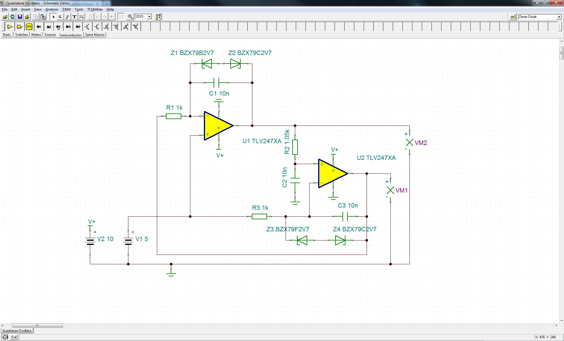
The circuit is close to sustaining oscillation. Changing resistor R2 to 10.5k will enable it to sustain oscillation. The original authors of the referenced note are no longer available for consultation. Oscillators of this type can be complex, as...
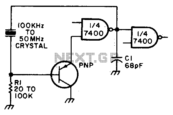
Adjust Rl for approximately 2 volts at the output of the first gate. Additionally, adjust Cl for optimal output. In the context of electronic circuit design, the output voltage of a gate, such as a logic gate or operational amplifier,...
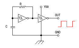
The hysteresis characteristic indicates that the voltage level transitions to high (H) when the input voltage of the inverter rises from 0 V, and the voltage level transitions to low (L) when the input voltage descends from +5 V....
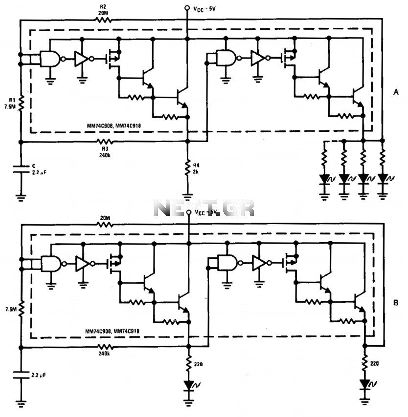
The driver in the package is configured as a Schmitt trigger oscillator (A), utilizing resistors R1 and R2 to create hysteresis. The inverting feedback timing components consist of resistor R3 and capacitor C, while resistor R4 serves as the...
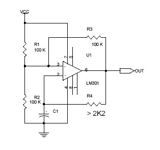
This circuit utilizes the Op-Amp LM301 to generate a simple square wave. The LM301 operates with a power supply range of 3 V to 36 V and can handle a maximum frequency of 325 kHz. The oscillation frequency is...
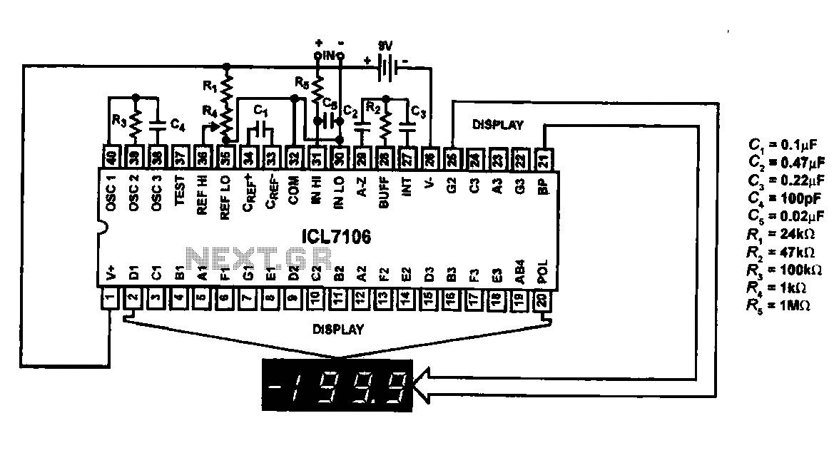
This circuit utilizes the ICL7106 / ICL7107 chip to drive a liquid crystal display (LCD). In this configuration, the ICL7106 / ICL7107 functions as a signal measurement and analog-to-digital (A/D) converter. It detects an analog input signal, amplifies it,...