
Switched-capacitor-adc
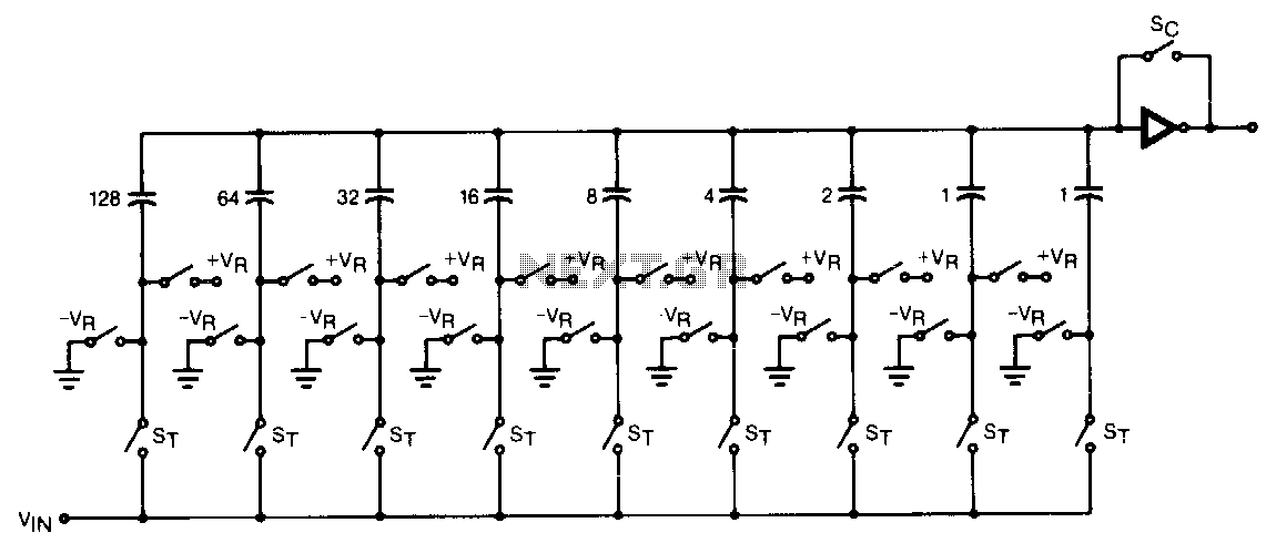
The CMOS comparator in the successive-approximation system determines each bit by examining the charge on a series of binary-weighted capacitors. In the first phase of the conversion process, the analog input is sampled by closing switch SC and all ST switches, and by simultaneously charging all the capacitors to the input voltage. In the next phase of the conversion process, all ST and SC switches are opened, and the comparator begins identifying bits by assessing the charge on each capacitor relative to the reference voltage. In the switching sequence, all eight capacitors are examined separately until all eight bits are identified, and then the charge-conversion sequence is repeated. In the first step of the conversion phase, the comparator evaluates the first capacitor (binary weight = 128). One pole of the capacitor is connected to the reference voltage, while the equivalent poles of all the other capacitors in the ladder are connected to ground. If the voltage at the summing node exceeds the trip point of the comparator—approximately half the reference voltage—a bit is recorded in the output register, and the 128-weight capacitor is switched to ground. If the voltage at the summing node is less than the trip point of the comparator, this 128-weight capacitor remains connected to the reference input throughout the remainder of the capacitor-sampling (bit-counting) process. The process is repeated for the 64-weight capacitor, the 32-weight capacitor, and so forth down the line until all bits are tested. With each step of the capacitor-sampling process, the initial charge is redistributed among the capacitors. The conversion process is based on successive approximation but relies on charge shifting rather than a successive-approximation register to count and weigh the bits from the most significant bit (MSB) to the least significant bit (LSB).
The CMOS comparator operates within a successive-approximation system that utilizes binary-weighted capacitors to perform analog-to-digital conversion. Initially, the system samples the analog input voltage by closing specific switches, SC and ST, ensuring that all capacitors are charged to the input voltage level. This process establishes a baseline for comparison in subsequent steps.
Once the input is sampled, the system transitions to the bit identification phase. During this phase, the comparator sequentially tests each capacitor's charge against a predefined reference voltage. The first capacitor in the sequence, with a binary weight of 128, is evaluated first. The comparator connects one terminal of this capacitor to the reference voltage and grounds the equivalent terminals of the remaining capacitors. The voltage at the summing node is then assessed. If it surpasses half of the reference voltage, a binary '1' is recorded in the output register, indicating that the 128-weight capacitor is significant for the current input voltage. Conversely, if the voltage is lower, the capacitor remains connected to the reference voltage for further evaluation.
This systematic approach continues down the line through the 64-weight, 32-weight, and so forth, ensuring that each capacitor is tested in turn. As each capacitor is evaluated, the charge is redistributed, allowing for accurate representation of the input voltage. The circuit effectively utilizes charge shifting techniques rather than traditional methods involving a successive-approximation register, thereby optimizing the conversion process from the most significant bit to the least significant bit. This method enhances efficiency and accuracy in digital representation of the analog input.The CMOS comparator in the successive-approximation system determines each bit by examining tbe charge on a series of binary-weighted capacitors. In tbe first phase of tbe conversion process, the analog input is sampled by closing switch SC and all ST switches, and by simultaneously charging all tbe capacitors to tbe input voltage.
In tbe next phase of tbe conversion process, all STand SC switches are opened and the comparator begins identifying bits by identifying the charge on each capacitor relative to the reference voltage. In tbe switching sequence, all 8 capacitors are examined separately until all 8 bits are identified, and tben tbe charge-convert sequence is repeated. In tbe first step of tbe conversion phase, tbe comparator looks at tbe first capacitor (binary weight = 128).
One pole of tbe capacitor is switched to the reference voltage, and tbe equivalent poles of all the otber capacitors on the ladder are switched to ground. If the voltage at the summing node is greater tban the trip point of the comparator-approximately 1/2 the reference voltage, a bit is placed in tbe output register, and tbe 128-weight capacitor is switched to ground.
If tbe voltage at tbe sununing node is less than tbe trip point of the comparator, this 128-weight capacitor remains connected to tbe reference input through tbe remainder of the capacitor-sampling (bit-counting) process. The process is repeated for tbe 64-weight capacitor, tbe 32-weight capacitor, and so forth down tbe line, until all bits are tested.
With each step of the capacitor-sampling process, the initial charge is redistributed among the capacitors. The conversion process is successive-approximation, but relies on charge shifting rather tban a successive-approximation register-and referenced/a-to count and weigh the bits from MSB to LSB.
🔗 External reference