
Switching-regulator
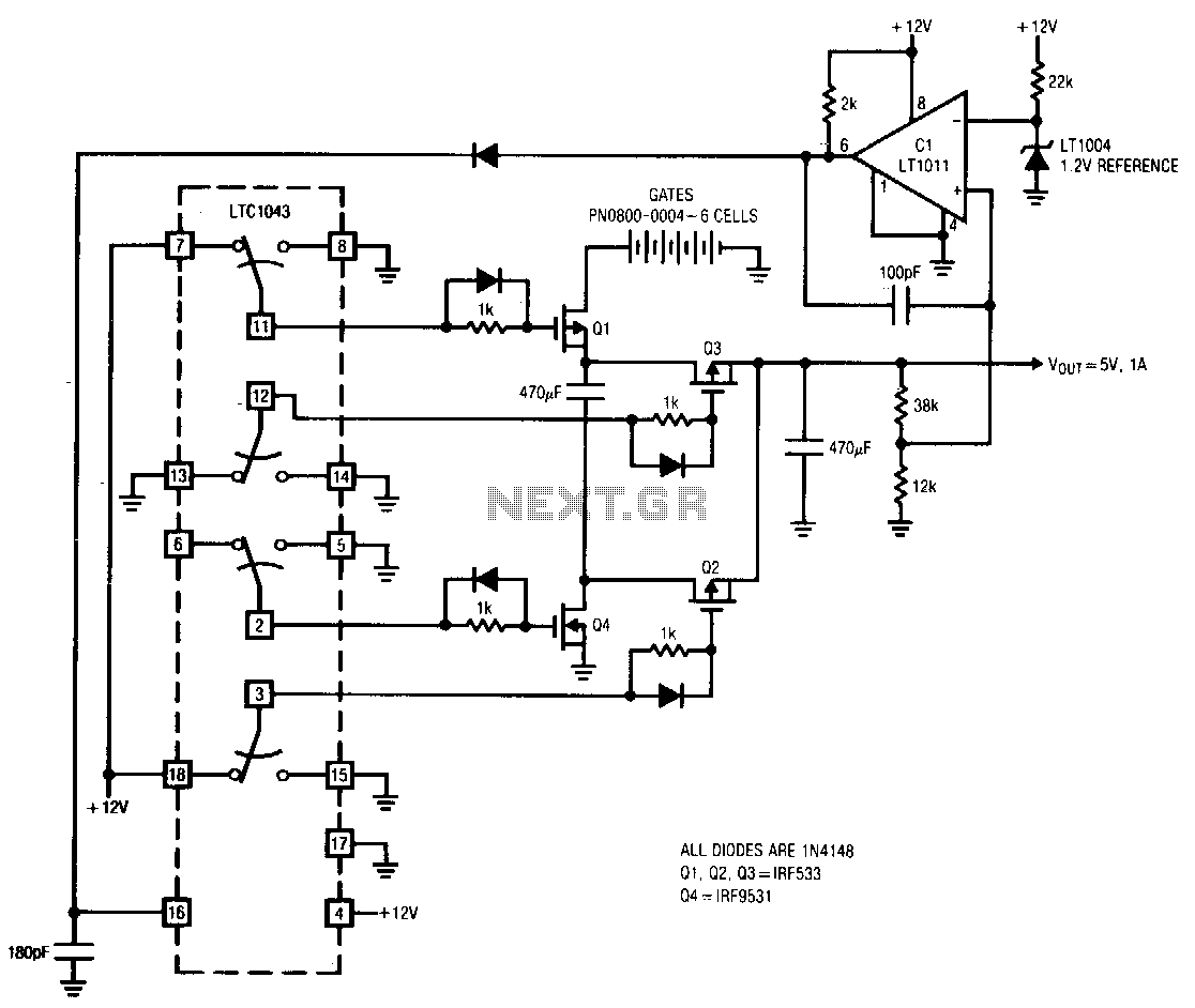
The LTC10432 switched-capacitor building block provides non-overlapping complementary drive to the Q1 to Q4 power MOSFETs. The MOSFETs are arranged such that C1 and C2 are alternately placed in series and parallel configurations. During the series phase, the +12 V battery's current flows through both capacitors, charging them and supplying load current. In the parallel phase, both capacitors deliver current to the load. Q1 and Q2 receive similar drive signals from pins 3 and 11. The diode-resistor networks enhance the non-overlapping drive characteristics, preventing simultaneous activation of the series-parallel phase switches. Normally, the output would be half of the supply voltage, but C1 and its associated components close a feedback loop, forcing the output to 5 V. In the series phase, the output rises rapidly. When the output exceeds 5 V, C1 triggers, causing the LTC1043 oscillator pin, trace D, to go high, which truncates the LTC1043's triangular-wave oscillator cycle. The circuit is then forced into the parallel phase, causing the output to gradually decrease until the next LTC1043 clock cycle begins. C1's output diode prevents the triangle down-slope from being affected, and the 100-pF capacitor ensures sharp transitions. The feedback loop regulates the output to 5 V by controlling the turn-off point of the series phase.
The LTC10432 circuit operates as a switched-capacitor voltage regulator, utilizing a pair of power MOSFETs (Q1 to Q4) to manage energy transfer between capacitors C1 and C2. The arrangement of the MOSFETs allows for efficient switching between series and parallel phases, which is critical for maintaining the desired output voltage and current characteristics. During the series phase, the capacitors are charged by the battery, effectively storing energy for later use. The non-overlapping drive provided by the LTC10432 ensures that only one phase is active at a time, preventing potential short circuits or inefficiencies that could arise from simultaneous switching.
The feedback mechanism involving C1 is integral to maintaining the output voltage at a stable 5 V. As the output voltage approaches this threshold, C1's role in the feedback loop becomes crucial, as it dictates when the system should transition from the series charging phase to the parallel discharging phase. This feedback control is essential for applications requiring precise voltage regulation, as it allows the circuit to respond dynamically to changes in load conditions.
The use of diode-resistor networks further enhances the circuit's performance by ensuring that the drive signals to the MOSFETs do not overlap, which could lead to undesirable effects such as shoot-through current. The inclusion of a 100-pF capacitor helps to improve the transient response of the circuit, allowing for quick adjustments to the output voltage as load conditions change. Overall, the LTC10432 is a sophisticated building block for switched-capacitor applications, providing both efficiency and reliability in voltage regulation tasks.The LTC10432 switched-capacitor building block provides nonoverlapping complementary drive to the Ql to Q4 power MOSFETs. The MOSFETs are arranged so that Cl and C2 are alternately placed in series and then parallel. During the series phase, the + 12 V battery"s current flows through both capacitors, charging them, and furnishing load current.
During the parallel phase, both capacitors deliver current to the load. Ql and Q2 receive similar drive from pins 3 and 11. The diode-resistor networks provide additional nonoverlapping drive characteristics, preventing simultaneous drive to the series-parallel phase switches. Normally, the output would be one-half of the supply voltage, but C1 and its associated components close a feedback loop, forcing the output to 5 V. With the circuit in the series phase, the output heads rapidly positive. When the output exceeds 5 V, Cl trips, forcing the LTC1043 oscillator pin, trace D, high; this truncates the LTC1043"s triangular-wave oscillator cycle.
The circuit is forced into the parallel phase and the output coasts down slowly, until the next LTC1043 clock cycle begins. Cl"s output diode prevents the triangle down-slope from being affected and the 100-pF capacitor provides sharp transitions.
The loop regulates the output to 5 V by feedback controlling the turn-off point of the series phase. 🔗 External reference
Related Circuits
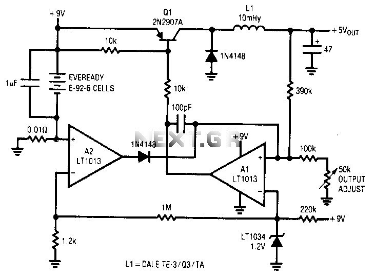
A simple battery-powered switching regulator provides 5 V output from a 9-V source with 80% efficiency and a 50 mA output capability. When Q1 is activated, its collector voltage increases, allowing current to flow through the inductor. This causes...