
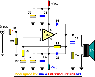
TDA2050 Audio Amplifier
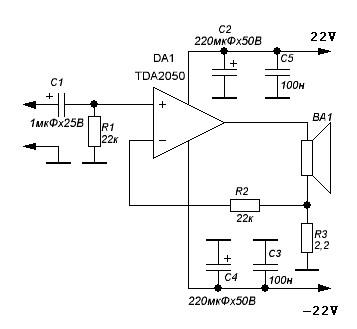
The TDA2050 audio amplifier is a high-performance integrated circuit designed for audio amplification applications. It features a robust output stage capable of delivering up to 14 watts of continuous power into an 8-ohm load, making it suitable for a variety of audio systems, including home audio, car audio, and professional sound systems.
The circuit design typically includes a power supply section that provides the necessary voltage levels for the TDA2050 to operate efficiently. The amplifier requires a dual power supply, usually ± 14V to ± 20V, to ensure optimal performance and headroom. The input stage is configured to accept audio signals from various sources, such as microphones or audio playback devices, with appropriate coupling capacitors to block any DC offset.
The feedback network, consisting of resistors R2 and R3, plays a crucial role in stabilizing the gain of the amplifier and ensuring linearity in the output signal. The reactance of the components, particularly at pin 4, is essential for maintaining the frequency response of the amplifier and preventing oscillations. Proper selection of these resistors and capacitors is critical for achieving the desired sound quality and amplifier performance.
Additionally, the circuit should include bypass capacitors near the power supply pins of the TDA2050 to filter out any high-frequency noise that may affect the performance. The output stage is typically connected to a speaker through a coupling capacitor, which helps to block DC components while allowing the AC audio signal to pass through.
Overall, the TDA2050 audio amplifier circuit is a well-engineered solution for high-fidelity audio applications, combining simplicity with effective performance, making it a popular choice among audio enthusiasts and engineers alike.TDA2050 Audio Amplifier circuit diagram. There is a current environmental protection: the signal from the output passes through the connecting cables and chains of the column (in this case takes into account the reactance of the circuit section of the 4th pin of the chip to R3), then the signal is removed from the NFB by R2 R3 and fed to the inver ted input circuits. 🔗 External reference
Related Circuits
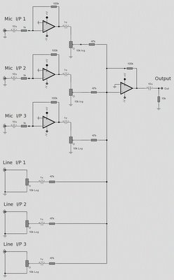
The microphone inputs are amplified approximately 100 times or 40 dB, with the total gain of the mixer, including the summing amplifier, reaching 46 dB. The microphone input is designed for microphones that produce an output of around 2...
The LM380 is a power audio amplifier designed for consumer applications. To minimize system costs, the gain is internally fixed at 34 dB. It features a unique input stage that allows for ground-referenced input signals. The output automatically self-centers...
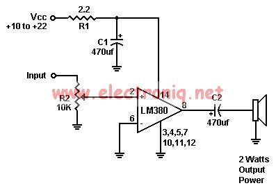
A simple audio amplifier can be designed using the LM380 along with a few external components. This amplifier features a wide supply voltage range, an input impedance of 150 kΩ, low distortion, and a current capability of 1.3 A. The...
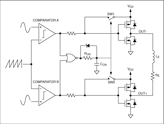
Ultra-low EMI, mono and stereo, Class D audio power amplifiers deliver Class AB performance while maintaining Class D efficiency. Maxim's spread spectrum modulation (SSM) combined with third-generation EMI reduction techniques minimizes EMI radiation by decreasing the high-frequency components of...

The circuit automatically lights a bulb upon the arrival of a telephone ring and simultaneously mutes the audio from the music system or TV while the telephone handset is off-hook. The lighting of the bulb not only indicates an...
A 2 x 18W Hi-Fi Stereo Power Amplifier is designed using two TDA2030 integrated circuits (ICs). This amplifier features excellent input sensitivity, low distortion levels, stable operation, and comprehensive protection against overloads and output short circuits. It can serve...