
The 567 FM demodulator circuit
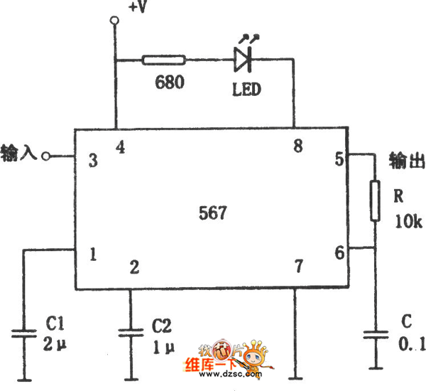
The 567 FM demodulator is a versatile integrated circuit designed for demodulating frequency-modulated (FM) signals. The circuit operates by utilizing phase-locked loop (PLL) techniques to extract the original audio or data signal from the modulated carrier wave. The central frequency, fo, which can be demodulated, is influenced by the values of the resistor (R) and capacitor (C) in the circuit, allowing for flexibility in tuning the circuit to different frequencies.
Pin 3 is designated for the input of the FM signal, which is then processed by the internal circuitry of the 567. The demodulated output signal can be accessed at pin 5, providing a clean representation of the original modulating signal. The filtering capacitor C1 is crucial in smoothing out the output signal, reducing noise and ensuring a clearer audio or data output.
Capacitor C2 plays a significant role in adjusting the bandwidth of the demodulator. By altering the value of C2, the user can modify the frequency response of the circuit, allowing for optimal performance depending on the characteristics of the incoming FM signal. A decrease in C2 results in a narrower bandwidth, which can enhance selectivity in environments with multiple overlapping signals. Conversely, increasing C2 broadens the bandwidth, which may be beneficial for receiving signals with a wider frequency deviation.
The 567 FM demodulator circuit is commonly used in various applications, including radio receivers, communication systems, and other electronic devices that require reliable FM signal demodulation. Its design emphasizes simplicity and effectiveness, making it a popular choice among engineers and hobbyists alike.In the figure is the 567 FM demodulator circuit. In the figure, the FM signal is input from 3-pin and the demodulated signal is output from 5-pin. The central frequency of the FM signal that the circuit can demodulate is: fo=1.1/RC. In the circuit, C1 is the filtering capacitor, C2 is the wide band adjusting capacitor, when C2 is going down, the band width o.. 🔗 External reference
Related Circuits
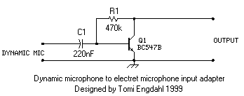
This is a simple microphone preamplifier circuit which you can use between your dynamic microphone and any equipment designed to work with an electret microphone (2 wire connection to electret capsule). This amplifier amplifies the low level signal to...
The output of this circuit should be connected to a high-impedance load, typically greater than 100K ohms, while noting that the impedance of capacitor C4 is approximately 3K ohms. A PNP transistor may also be utilized, requiring adjustments to...
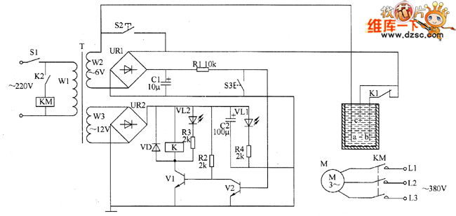
The liquid level controller circuit comprises a power supply circuit and a level detection control circuit, as illustrated in the accompanying chart. The power supply circuit includes a power switch (S1), a power transformer (T), bridge rectifiers (UR1, UR2),...
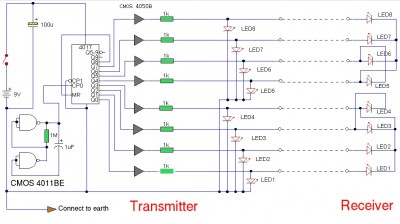
The LAN tester circuit can also test cables such as telephone, coaxial, LAN, and others. This circuit uses LEDs as the main indicator device. The LAN tester circuit is designed to verify the integrity and functionality of various types of...
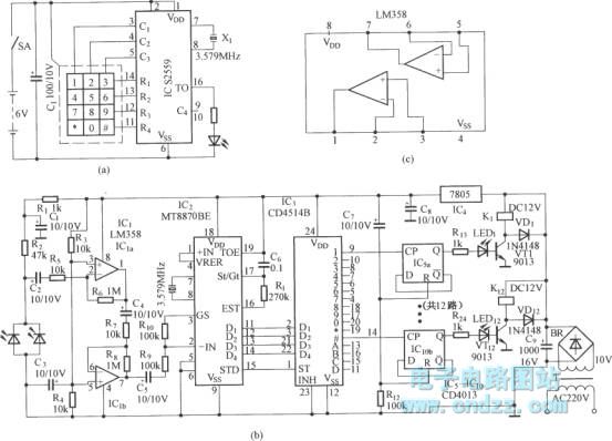
Figure (a) illustrates an infrared emission circuit composed of a 12-key keyboard and an S2559. Figure (b) displays a DTMF decoder circuit along with a channel control circuit utilizing the MT8870. Figure (c) presents a voltage amplifier circuit constructed...
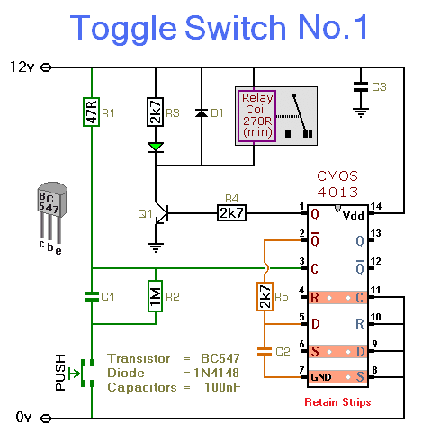
This simple circuit will energize and de-energize a relay with the push of a button. Pressing the button once will energize the relay, while pressing it a second time will de-energize the relay. The accompanying circuit provides a solid...
Warning: include(partials/cookie-banner.php): Failed to open stream: Permission denied in /var/www/html/nextgr/view-circuit.php on line 713
Warning: include(): Failed opening 'partials/cookie-banner.php' for inclusion (include_path='.:/usr/share/php') in /var/www/html/nextgr/view-circuit.php on line 713