
The Colpitts Oscillator
The Colpitts oscillator design is notable for its simplicity and effectiveness in generating high-frequency oscillations. The circuit's configuration allows for precise control over the frequency of oscillation through the careful selection of the capacitors and inductor. The relationship between the capacitors ensures that the feedback necessary for sustained oscillation is maintained without introducing instability due to mutual inductance.
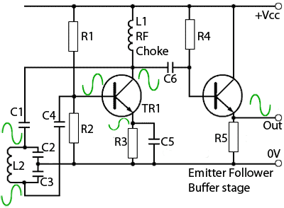
In practical applications, the Colpitts oscillator can be used in various RF circuits, including signal generators and frequency synthesizers. Its ability to produce a clean sine wave output makes it suitable for applications where signal integrity is critical. The design also allows for easy integration into larger circuits, with the emitter follower buffer providing a means to drive subsequent stages without loading the oscillator itself.
The implementation of automatic class C biasing further enhances the performance of the oscillator, allowing it to operate efficiently across a range of conditions. This characteristic is particularly beneficial in communication systems where signal fidelity and frequency stability are paramount.
Overall, the Colpitts oscillator serves as a foundational component in many electronic systems, providing a reliable source of oscillation with good frequency stability and waveform quality.A typical Colpitts oscillator design. This circuit is very similar in operation to the Hartley oscillator described in Oscillators Module 2. 1 but the Colpitts LC tank circuit consists of a single inductor and two capacitors. The capacitors form in effect, a single `tapped` capacitor instead of the tapped inductor used in the Hartl
ey. The values of the two capacitors (connected in series) are chosen so their total capacitance in series(CTOT), is given by: This gives the total capacitance necessary for the tank circuit to achieve parallel resonance at the required frequency. The frequency of oscillation is given by the same formula as for the Hartley oscillator: The individual values of C2 and C3 are chosen so that the ratio of the values produces the necessary proportion of feedback signal.
However, the ratio of voltages across two capacitors in series is in inverse proportion to the ratio of the values, i. e. the smaller capacitor has the larger signal voltage across it. The main advantage of the Colpitts arrangement, is that the single inductor in the tuned circuit removes the effect of any mutual inductance between two coils where the alternating magnetic field built up around one inductor induces a current into the their inductor.
This would affect the total inductance of the coils and so changes the resonant frequency of the tuned circuit. The circuit in Fig. 2. 3. 2 is the Colpitts equivalent of the Common Emitter Hartley Oscillator described in Oscillators Module 2.
1 (Fig. 2. 1. 4). It uses a common emitter amplifier, and as the tuned (tank) circuit tapping point in this configuration is connected to ground, the tank circuit produces anti-phase waves at top and bottom of L2, which ensures the correct phase relationships for positive feed back between collector and base. The feedback is applied to the base via C1, which also acts as a DC block, preventing the higher voltage on L1 upsetting the base bias voltage.
Note that the tank circuit (L2, C2 and C3)is connected to the supply rail (+Vcc) via L1. If the tank circuit were connected directly to the supply there could be no anti-phase AC signal present at the top of the tank circuit, due to the DC supply being heavily decoupled by large capacitors in the DC Ppower supply. An RF choke (L1) having a high impedance at the frequency of oscillation is therefore included between the tuned circuit and the supply.
This allows for a signal voltage for feedback purposes to be developed across L1. Automatic class C bias is used, with the emitter in this circuit only partially decoupled by a small value of C5 to give the sliding bias` previously described. The Colpitts oscillator, like the Hartley is capable of giving an excellent sine wave shape, and also has the advantage of better stability at very high frequencies.
It can be recognised by always having a "tapped capacitor" Sine wave oscillator design is complicated by the fact that any load placed on the output, by circuits that the output is supplying, effectively places a damping resistance across the tank circuit. As well as reducing the amplitude of the oscillator output by having the effect of reducing the Q factor of the tuned tank circuit, this can adversely affect both the wave shape and the frequency stability of the oscillator waveform.
A common solution is to feed the oscillator output into an emitter follower buffer amplifier, as shown in Fig. 2. 3. 2. The oscillator section of this circuit is a slightly different version of the Colpitts oscillator in shown in Fig.
2. 3. 1. The RF choke is now the load impedance for TR1 and the tank circuit is isolated from TR1 by two DC blocking capacitors, C1 and C4. Therefore this version of the Colpitts oscillator uses a tuned feedback path ( Method 1 in Oscillators Module 1.
1) rather than a tuned amplifier ( Method 2 ) as in Fig. 2. 3. 1 The emitter follower stage (R4, TR2 and R5) has a very hig 🔗 External reference
Related Circuits
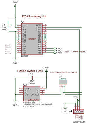
The SX 28 internal oscillator is not that fast, so an external oscillator can be hooked up to the processor as shown in the diagram to increase the operation cycles per second. The SX 28 microcontroller is designed with an...
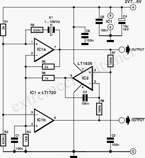
A simple crystal oscillator can be constructed using a comparator from the LT1720/LT1721 series; however, this design may encounter several inherent limitations and issues. While the LT1720/LT1721 provides the correct logic output when one input falls outside the common...

This design circuit features a simple, cost-effective amplitude-stabilized phase-shift sine wave oscillator that requires one integrated circuit (IC) package, three transistors, and operates from a single power supply. The circuit incorporates an RC network configured for phase shift, oscillating...
A single transistor is utilized to create a simple phase shift oscillator. The output produced is a sine wave with a distortion level of approximately 104. The purity of the sine wave can be improved by incorporating a variable...
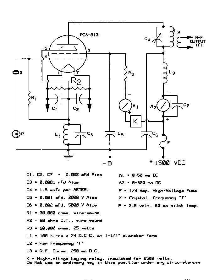
The single-813 crystal oscillator transmitter, designed by RCA, was showcased in an advertisement on the back page of a 1938 "QST" magazine and published in the RCA HamTips bulletin, volume 1, number 4, dated December 1938. This transmitter delivers...
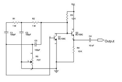
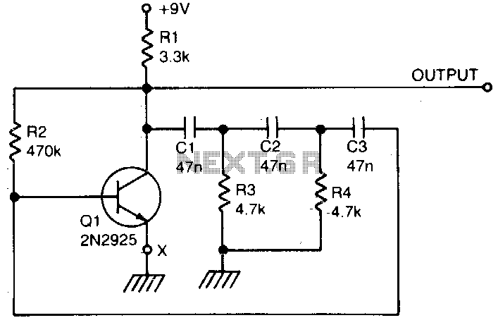
This circuit is a sine wave oscillator with a frequency range from 5 Hz to 5 kHz. The capacitors C1, C2, and C3, with a combined value of 100 pF, produce a frequency of 5 kHz. To achieve different...
Warning: include(partials/cookie-banner.php): Failed to open stream: Permission denied in /var/www/html/nextgr/view-circuit.php on line 713
Warning: include(): Failed opening 'partials/cookie-banner.php' for inclusion (include_path='.:/usr/share/php') in /var/www/html/nextgr/view-circuit.php on line 713