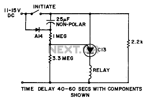
Timing-threshold-and-load-driver

Power is applied to the circuit with the initiate switch open. The 25 µF capacitor charges through the A14 diode, or an equivalent, and a 2.2 kΩ resistor to the full supply voltage. When the initiate switch is closed, the low side of the capacitor is suddenly raised to +12 V. This raises the diode side of the capacitor to approximately +24 V. The capacitor immediately begins discharging through the series-connected 1 MΩ and 3.3 MΩ resistors. Eventually, the C13 gate becomes forward biased, the device turns on, and it applies power to the relay. The delay is virtually independent of the supply voltage.
The described circuit operates by utilizing a capacitor to create a delayed response in activating a relay. Initially, when the initiate switch is in the open position, the capacitor (25 µF) is charged through a diode (A14 or equivalent) and a resistor (2.2 kΩ). This charging process allows the capacitor to reach the full supply voltage, which is critical for the subsequent operation of the circuit.
Upon closing the initiate switch, the voltage at the low side of the capacitor is instantaneously elevated to +12 V. This sudden change in voltage causes the high side of the capacitor, connected through the diode, to rise to approximately +24 V. The rapid discharge of the capacitor occurs through two resistors connected in series (1 MΩ and 3.3 MΩ). The discharge path is essential as it controls the timing of the voltage drop across the capacitor.
As the capacitor discharges, the voltage across it decreases, leading to the eventual forward biasing of the gate of the device labeled C13. This condition triggers the device to turn on, resulting in the application of power to the relay. The relay serves as the output component that performs a specific function in the circuit, such as switching on a load or controlling another part of the system.
The delay between the closing of the initiate switch and the activation of the relay is noteworthy as it is largely unaffected by variations in supply voltage. This characteristic can be advantageous in applications where consistent timing is required regardless of supply fluctuations. Overall, this circuit design efficiently utilizes a capacitor's charge and discharge properties to implement a controlled delay in relay activation.Power is applied to the circuit with the initiate switch open. The 25-JtF capacitor charges through the A14, or equivalent, diode and 2.2-KO resistor to full supply voltage. When the initiate switch is closed, the low side of the capacitor is suddenly raised to +12 V. This raises the diode side of the capacitor to approximately +24 V. The capacitor immediately begins discharging through the seriesconnected 1 and 3.3-MO resistors. Eventually, the C13 gate becomes forward biased, the device turns, and it applies power to the relay. The delay is virtually independent of supply voltage.