
Touch detecting Switches
A finger touching the pad dramatically increases its capacitance and the larger capacitance cannot discharge through R5 fast enough to allow IC2:C to switch, so its output pulses go away and its output stays low. With the charging pulses gone, C4 soon discharges through R7 and when its voltage falls below the threshold of IC2:D, this gate's output switches high, which represents the switch being "on".
Some touch switch designs tend to be "bouncy", which is to say that they may toggle rapidly between "on" and "off" when the pad is in that gray area between touched and, uh ... untouched. This design gets rid of the "on" bounce with short delays before responding - a finger has to be on the pad for 1mS or so before the output changes state.
To debounce the "off" cycle, the clock is turned off briefly when a switch is released. In the circuit above, diodes D3 and D6 and resistor R6 form an OR circuit that causes the voltage across R6 to be high when any output is high. This voltage goes low when a switch is released, causing the monostable comprising C3, R4 and IC1:D to produce a short pulse that momentarily kills the clock by gating it off in IC1:C. While the clock is stopped the switch will read as "off" even if the finger is pressed back on the pad.
This circuit is pretty forgiving of supply voltages. In the PDS, it was run from a 6V battery but anything from 5V to 18V should work fine.
In the PDS, the touch pads were copper land areas about 1/4" X 3/4" etched on the edge of the circuit board that also mounted the rest of the electronics. The pads were covered with epoxy ink to protect them and also legend their function. It looked like this. In prototype form, the pads can be covered by a strip of cellophane tape. It's not a good idea to touch the bare plate with your finger because this can produce unreliable operation. Changes in the size of the pads may require adjustments of the time constants.
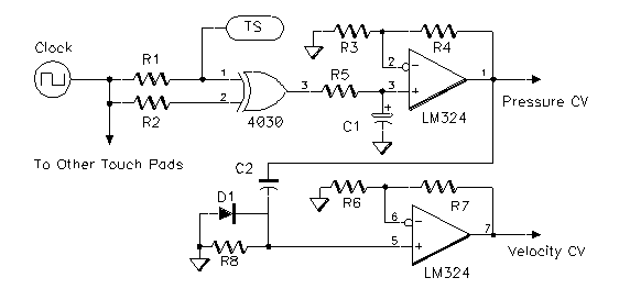
The Pressure (Velocity) sensitive version The circuit shown below measures this change in capacitance and converts it to a Pulse Width Modulated signal. The clock shown in the drawing is the same clock used in the earlier touch switches, but its frequency may need to be adjusted up or down for best operation. The clock signal is coupled to the two inputs of a 4030 CMOS ExOR gate by R1 and R2. When no finger is touching the pad associated with R1, the parasitic capacitance at the two inputs is about the same so the clock signal is more or less the same at both inputs. Since an ExOR gate has a high output only when the two inputs are different, the output stays low even though the two inputs are clocking. As the finger is brought up to the pad and capacitance increases, the phase of the input to pin 1 (with the touch pad) begins to lag. As the two inputs get more different the output of the gate produces a pair of pulses (one on the leading edge of the clock signal and the other on the trailing edge) and the width of the pulses increases. R5 and C1 integrate this variable width pulse to extract its average dc value. This voltage is amplified by the voltage follower with gain consisting of IC1, R3 and R4 and is available as a Pressure Control Voltage.One of the unusual features of the out-of-production Programmable Drum Set was its use of touch switches for control. Like most touch switches, these detect the difference in the capacitance of a plate when it is being touched by a finger versus the parasitic capacitance of the plate alone.
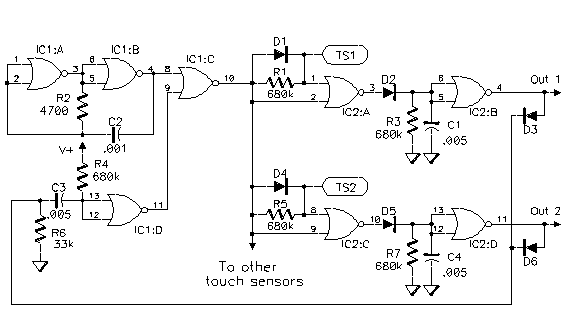
The capacitance added by touching the plate is detected using a square wave oscillator. In the diagram below IC1:A and IC1:B, two gates from a 4001 CMOS Quad NOR IC, form an astable multivibrator with a 50kHz frequency as determined by the time constant of R2 and C2. The square wave output is buffered by IC1:C and used to drive a group of touch switches. Only two switch plates - TS1 and TS2 - are shown in the illustration, but in the PDS, 16 touch switches were excited by this one clock.
When the clock waveform is high, the capacitance of the sensing plate (TS2, for example) quickly charges through the forward biased diode D4 whether the pad is being touched by a finger or not. When the clock is low, the capacitor discharges through R5 and with no finger present the voltage quickly falls below the threshold required to switch IC2:C.
Because of the inversion of the gate, it's output is a series of positive pulses at the clock frequency. The pulses quickly charge C4 through D5, but the C4 - R7 time constant is long enough that C4 can't discharge between pulses, so the output of IC2:D (which is the "switch" output) is low when there is no finger on the pad.
A finger touching the pad dramatically increases its capacitance and the larger capacitance cannot discharge through R5 fast enough to allow IC2:C to switch, so its output pulses go away and its output stays low. With the charging pulses gone, C4 soon discharges through R7 and when its voltage falls below the threshold of IC2:D, this gate's output switches high, which represents the switch being "on".
Some touch switch designs tend to be "bouncy", which is to say that they may toggle rapidly between "on" and "off" when the pad is in that gray area between touched and, uh ... untouched. This design gets rid of the "on" bounce with short delays before responding - a finger has to be on the pad for 1mS.
or so before the output changes state. To debounce the "off" cycle, the clock is turned off briefly when a switch is released. In the circuit above, diodes D3 and D6 and resistor R6 form an OR circuit that causes the voltage across R6 to be high when any output is high. This voltage goes low when a switch is released, causing the monostable comprising C3, R4 and IC1:D to produce a short pulse that momentarily kills the clock by gating it off in IC1:C.
While the clock is stopped the switch will read as "off" even if the finger is pressed back on the pad. This circuit is pretty forgiving of supply voltages. In the PDS it was run from a 6V battery but anything from 5V to 18V should work fine. In the PDS, the touch pads were copper land areas about 1/4" X 3/4" etched on the edge of the circuit board that also mounted the rest of the electronics.
The pads were covered with epoxy ink to protect them and also legend their function. It looked like this. In prototype form, the pads can be covered by a strip of cellophane tape. It's not a good idea to touch the bare plate with your finger because this can produce unreliable operation. Changes in the size of the pads may require adjustments of the time constants. Disclaimer: I have not built this pressure sensitive touch switch circuit so it may have unforeseen problems - in the real world of design this often happens, at least to me.
The idea exploits the fact that the capacitance produced by the finger on the pad is roughly proportional to the force of the finger on the pad. The Pressure (Velocity) sensitive version The circuit shown below measures this change in capacitance and converts it to a Pulse Width Modulated signal.
The clock shown in the drawing is the same clock used in the earlier touch switches, but it’s frequency may need to be adjusted up or down for best operation. The clock signal is coupled to the two inputs of a 4030 CMOS ExOR gate by R1 and R2. When no finger is touching the pad associated with R1, the parasitic capacitance at the two inputs is about the same so the clock signal is more or less the same at both inputs.
Since an ExOR gate has a high output only when the two inputs are different, the output stays low even though the two inputs are clocking. As the finger is brought up to the pad and capacitance increases, the phase of the input to pin 1 (with the touch pad) begins to lag.
As the two inputs get more different the output of the gate produces a pair of pulses (one on the leading edge of the clock signal and the other on the trailing edge) and the width of the pulses increases. R5 and C1 integrate this variable width pulse to extract it’s average dc value. This voltage is amplified by the voltage follower with gain consisting of IC1, R3 and R4 and is available as a Pressure Control Voltage.
🔗 External reference
Related Circuits
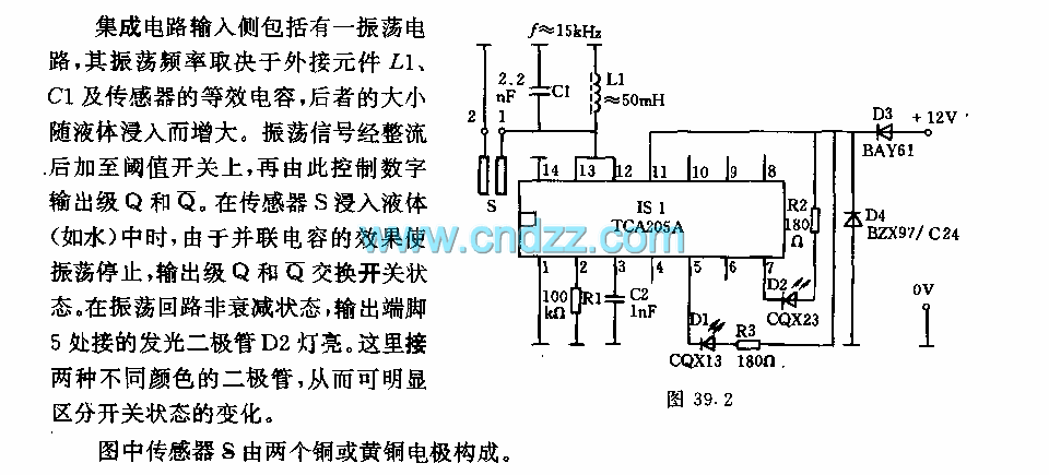
The integrated circuit input side contains an oscillating circuit, where the oscillation frequency is determined by the external components L1, C1, and the sensor's equivalent capacitance. The equivalent capacitance increases as the sensor is immersed in liquid. The oscillating...
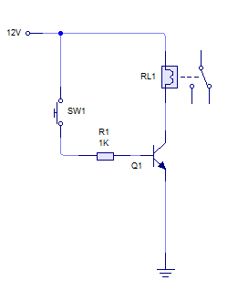
A relay is activated by grounding the low side using an NPN transistor. A pushbutton is intended to operate the transistor, thereby energizing the relay for approximately 500 milliseconds before deactivating it, while ignoring any continuous button press. Although...
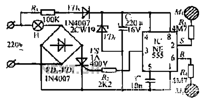
220V AC by Ri buck, Diao. C1 chain ferry flood ear, shouted for the regulator to 12V make C collapse. The film hand touch under ridicule the MT electrode films, clutter body. More: induction signal sent by See Cutting...
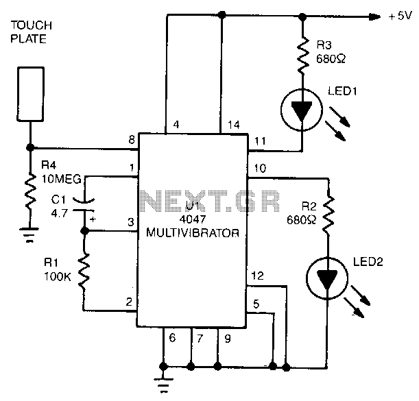
The 4047 is configured as a monostable multivibrator circuit, also known as a one-shot, which is triggered by a negative transition of the signal applied to its pin 6 input. The duration of the multivibrator's output pulse is determined...
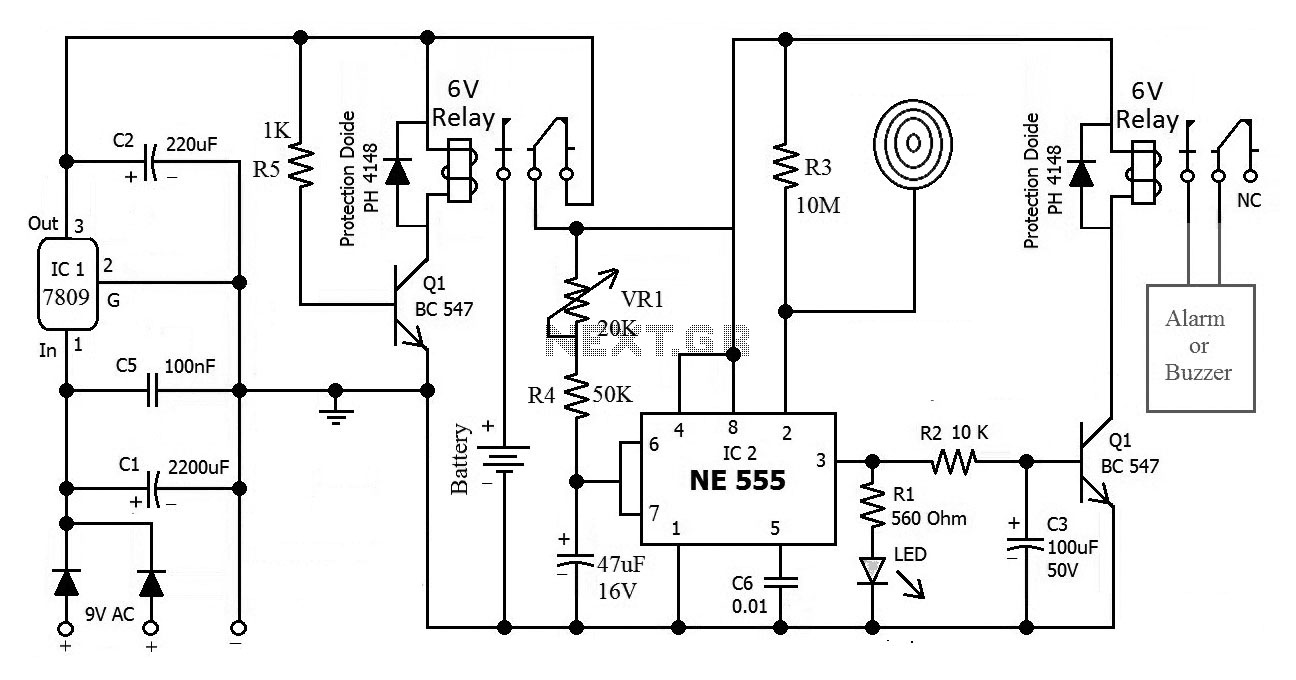
This is the circuit diagram of a touch-activated alarm system that remains operational during power outages. The alarm system is triggered when someone touches the designated touch plate. A notable feature of this circuit is the automatic battery activator,...
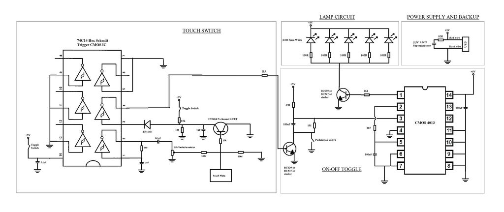
A touch switch for a USB-powered desk lamp is malfunctioning. The circuit diagram, layout, and pictures are provided below. The design incorporates circuits sourced from two websites, specifically the fourth circuit. The output of the touch switch is connected...
Warning: include(partials/cookie-banner.php): Failed to open stream: Permission denied in /var/www/html/nextgr/view-circuit.php on line 713
Warning: include(): Failed opening 'partials/cookie-banner.php' for inclusion (include_path='.:/usr/share/php') in /var/www/html/nextgr/view-circuit.php on line 713