
Touch switch circuit
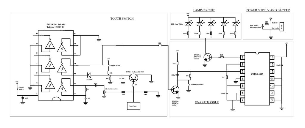
Concerns have been raised regarding potential issues with the circuit design. If problems persist, it is recommended to disconnect the 12V supply and the 10k resistor between the JFET and the inverter, and to incorporate a current-limiting resistor of approximately 1k ohms, as illustrated in the accompanying image. The positive voltage does not affect the inverter, while the absence of voltage also fails to influence its state; however, applying voltage does cause the inverter to change state. Currently, the inverter is receiving neither voltage nor a positive supply.
The schematic is difficult to interpret, with connections and junctions lacking clarity. The configuration of the JFET is ambiguous, as it is unclear which terminal is the source and which is the drain, raising concerns about correct connections. It is inadvisable to make assumptions in troubleshooting circuit failures. Additionally, the on/off status of the switches is not discernible. In the schematic, all wires that cross are connected, except for the one leading from pin 3 of the CMOS 4013. The layout diagram and pictures may assist in determining the correct orientation of the JFET.
The schematic used for the circuit construction is provided, but the source and drain of the JFET were not identifiable, leading to an assumption that the drain is connected to ground. Verification is needed to confirm this assumption and whether flipping the JFET is necessary. Both toggle switches are closed, serving to deactivate the touch functionality when not in use. The pushbutton switch is normally open and acts as a backup if the touch functionality fails, performing the same role as the parallel transistor, which controls the CMOS 4013 operation.
The schematic is noted to be challenging to read, with connections requiring clearer representation. The JFET's source and drain orientation must be verified, as assumptions can hinder troubleshooting efforts. The on/off positions of the switches are also unclear. A voltmeter should be used to ensure that traces are completely severed. It is important to confirm whether the pushbutton switch is designed to be "normally off" when momentarily activated, as tactile switches can be ambiguous in terms of which pins are internally connected. Adjustments may be necessary based on the orientation of the components.
In summary, the circuit design for the touch switch involves critical components such as a JFET, CMOS inverter, and toggle switches, all of which require careful consideration for proper functionality. The clarity of the schematic and component connections is essential for successful troubleshooting and operation of the USB-powered desk lamp.A touch switch for a USB powered desk lamp, and the touch switch isn`t working. The circuit diagram, layout and pictures are below. I used the circuits from the following two websites to design the circuit: the 4th circuit. I`ve joined the output of the touch switch to a transistor that should activate the toggle. But the outputof the touch switch appears to be constantly on. Can anyone see a problem with my circuit design or circuit Then if it still gives you trouble, pull the 12 + volts and 10 K between the Jfet and the inverter and put a current limiting resistor about 1K as in my pic. From the picks + volts does not do anything for the inverter and no volts does nothing for the inverter.
However volts does make the inverter change state. Right now the inverter is getting no volts or + volts. First your schematics are hard to read joints and jumps should be pronounced like this pic. Also on your jfet I cannot tell your source from your drain and whether it is connected correctly, now I could assume however that is a bad thing to do when trying to find out why a circuit doesn`t work. Also cannot tell the on or off position of your switches. All the wires that crossover in the schematic are joined except for the one from pin 3 of the CMOS 4013.
Could you use the layout diagram and pictures to figure out the orientation of the JFET Below is the schematic I used to make the circuit, and when I was making the circuit I couldn`t tell where the source or drain was, so I guessed that the drain would be the one connected to ground. Is this correct Should I try flipping the JFET around Both toggle switches are closed, they are just used to turn of the touch part of the circuit when not in use.
The pushbutton is normally open and is only used as a backup if the touch doesn`t work. It does the same thing as the transistor that it is parallel to, which is to make the CMOS 4013 turn on or off. First your schematics are hard to read joints and jumps should be pronounced like this pic. Also on your jfet I cannot tell your source from your drain and whether it is connected correctly, now I could assume however that is a bad thing to do when trying to find out why a circuit doesn`t work.
Also cannot tell the on or off position of your switches. Check with a voltmeter that your traces were cut completely. Is the pushbutton switch one that needs to be "normally off" when you have a mometary "normally on" also, you really can`t tell with those tactile switches which sides are shorted - 2 pins on one side are connected internally. You may have to turn the thing the other way. 🔗 External reference
Related Circuits
A daily switching power supply primarily provides direct current (DC) power to electronic devices. The required DC voltage for electronic devices typically ranges from several volts to over ten volts, while the input voltage from the mains supply is...

The Panasonic M12H switching power supply circuit is utilized in Panasonic models such as TC-230H, TC-2030DHN, TC-830D, and TC-840D. The circuit operates with an oscillation frequency that generates approximately 300V DC voltage at C836. The T801 transformer is involved...
Unfortunately, there is no breadboard available for testing; however, modifications can be made to the PCB. The 1K potentiometer has been removed until the strobe functionality can be established. The circuit in question appears to involve a strobe light mechanism,...

An adjustable pulse generator circuit is presented, which produces a periodic signal with independently adjustable pulse widths. The electrical path allows for modifications to the signal period through the adjustment of RP1. Additionally, RP2 can be altered to change...

A DIY RF decibel (or power) meter is an essential instrument in any radio workshop. However, accurate, wideband models can be quite costly. A DIY RF decibel meter serves as a valuable tool for measuring the power levels of radio...
The individual is new to electronics but enjoys experimentation. They plan to create a small guitar amplifier based on a 30 Watt design, specifically the single 12VDC version referenced in comments. The intention is to incorporate a preamplifier to...
Warning: include(partials/cookie-banner.php): Failed to open stream: Permission denied in /var/www/html/nextgr/view-circuit.php on line 713
Warning: include(): Failed opening 'partials/cookie-banner.php' for inclusion (include_path='.:/usr/share/php') in /var/www/html/nextgr/view-circuit.php on line 713