
Touch Switch Monostable/Timer with 555 IC
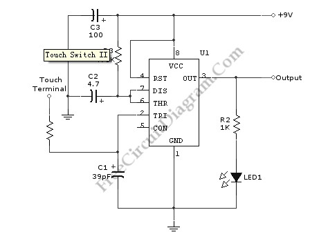
The touch switch circuit operates based on a timing mechanism that leverages the charging and discharging characteristics of capacitor C2 in conjunction with the resistance offered by R3. The circuit typically includes a power source, a microcontroller or a timer IC, a touch-sensitive input, C2, R3, and an output device such as an LED or relay.
When the touch switch is activated, the capacitor C2 begins to charge through resistor R3. The time constant of the RC charging circuit, defined as τ = R3 * C2, determines the duration for which the output remains active. The output will remain in the ON state for a period proportional to this time constant.
For practical implementation, the choice of capacitor and resistor values should consider the desired ON duration and the overall circuit response time. For instance, if a longer ON time is required, selecting a larger capacitor or a higher resistance value will achieve this. Conversely, a smaller capacitor or resistor will reduce the ON time.
It is also essential to consider the input characteristics of the touch switch, which may involve additional components like a pull-down resistor to ensure stable operation and prevent false triggering. The output stage may include a transistor or a relay to control higher power loads, providing isolation between the low-power control circuit and the load.
In conclusion, the touch switch circuit is a versatile design that can be adapted for various applications by adjusting the timing components. Proper selection of C2 and R3 is crucial for achieving the desired operational characteristics.Using the given values as shown in the schematic diagram, this circuit has timed ON period of 4 seconds. The value of C2 and R3 determines the ON time, increasing the value of C2 or R3 will increase the ON time.
The ON time is decreased if the value of C2 or R3 is decreased. A schematic diagram of a touch switch circuit is shown below. This circuit consist.. 🔗 External reference
Related Circuits
This document outlines a basic circuit designed to power high impedance, high voltage, low current devices such as electroluminescent (EL) backlights and fluorescent tubes. The project originated from the need for a simple yet flexible inverter circuit for an...
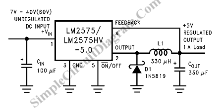
Switching Regulator for High Power Efficiency. When it is necessary to convert a high voltage to a significantly lower voltage, a switching regulator is the optimal choice. A switching regulator is an essential component in modern power management systems, particularly...

This is a simple automatic light switch circuit designed for bedrooms. After construction, connect the input terminals of this circuit in parallel to the existing light fixture. The automatic light switch circuit operates using a photoresistor (LDR) and a transistor...
When the touch switch SI is activated, resistor R4 is driven high, causing the control voltage to rise, which latches the switch. Conversely, when switch S2 is activated, resistor R4 goes low, resulting in a decrease in the control...
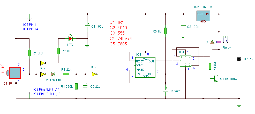
This is a single-channel (on/off) universal switch that can be used with any infrared remote control operating within wavelengths of 850-950 nm. The single-channel universal switch functions as a simple on/off control mechanism, allowing users to operate electronic devices remotely...
The 555 timer is recognized as one of the most versatile and widely used integrated circuits globally. One of its potential applications is as a simple inverting Schmitt trigger. The 555 timer can be configured in various modes, including monostable,...