
tr switch
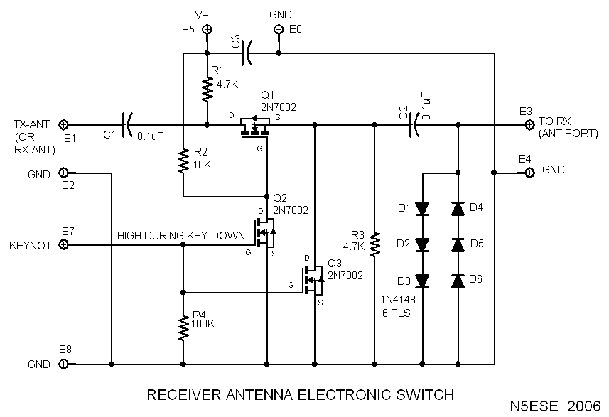
The universal QRP T/R switch circuit operates by utilizing the unique characteristics of MOSFETs to manage RF signals effectively. The primary components include three 2N7000 MOSFETs (Q1, Q2, and Q3) and an array of diodes. Q1 is responsible for switching the connection between the receiver's antenna input and the antenna itself. During the receive mode, Q1 is activated, allowing the RF signals from the antenna to reach the receiver. Conversely, during transmission, Q1 is turned off, and Q3 is activated to short the receiver input, thus preventing any RF energy from damaging the receiver.
The design also incorporates a diode array that acts as a voltage limiter, ensuring that any signals that inadvertently reach the receiver during transmission do not exceed 4 volts peak-to-peak. This feature is crucial for protecting sensitive receiver components from potential damage caused by high voltage spikes. The control mechanism for the T/R switch is managed by Q2, which serves as a buffer that responds to control signals from the KEYNOT port. This control signal is typically generated by the transmitter or control circuitry, allowing for seamless integration into various QRP setups.
The overall design emphasizes simplicity and reliability, making it an ideal solution for amateur radio operators looking to enhance their QRP systems. The T/R switch circuit can be easily implemented on a PCB, with careful attention to the layout to minimize parasitic capacitance and inductance, ensuring optimal performance at the desired frequency ranges. The universal nature of this T/R switch allows it to be adapted for a wide range of applications, making it a valuable addition to any QRP enthusiast's toolkit.The project I present here is my attempt at a universal QRP T/R switch. The idea is to take care of the essentials, so that any QRP (i. e. , less than 10W) receiver *AND* CW transmitter can be connected, and work seamlessly. These are what I considered the "essentials" to be: The operational scenario would be as follows, and could easily be applied to any QRP transmitter (or transceiver used as a transmitter) and any receiver (or transceiver used as a receiver). But the device is especially designed to accommodate a simple transmitter and receiver, each having few embellishments, and requiring none.
Operationally, here`s how a typical case would work: When Steve Weber, KD1JV, used three 2N7000 power MosFETs in the final of his AT Sprint transceiver, and managed to produce 6 watts with same (4W at 20 Meters), it really opened my eyes to these little devices. I had always thought of these as audio or power-control devices, but now I began to think in a different direction.
One thing that immediately occured to me is that these devices might be configured in such a manner as to provide an "on/off" switch to RF energy between the transmit line and the receiver`s antenna input. They could additionally provide protection to the receiver, by shunting any unwanted energy that might make it as far as the receiver`s antenna input.
This led to some experimenting in SPICE, and eventually to the following essential T/R switch circuit: Let`s review the schematic. The transmit signal is tapped at the transmitter output - the transmitter remains connected to the antenna at all times - and arrives at the left "TX-ANT" port.
Q1 serves to connect the receiver antenna port (right, "TO RX") to the antenna (during receive), or isolate it (during transmit). Because Q1 does not completely isolate the transmit signal (because of device leakage), Q3 serves to short the receiver input during transmit.
The array of diodes clips any signals that may arrive during receive periods, and limits any voltage presented to the receiver antenna input to about 4 Volts peak-to-peak. Q2 is the control buffer for Q1. A "high" control signal to the "KEYNOT" port (from the control circuitry, representing the 🔗 External reference
Related Circuits
Closing the switch S allows the AC positive half-cycle to flow through diode VDI and resistor R, causing the SCR to open simultaneously at both ends of the capacitor C, which becomes fully charged. During this phase, the positive...
At times, it is quite frustrating to see street lights remaining switched on even during broad daylight. The current circuit for an automatic night light can effectively address this issue. This article explains how to construct such a system....
This is an intriguing 555 timer circuit designed to entertain and engage individuals while studying electronics in educational settings. Commonly referred to as a clap switch circuit, it operates as a sound-controlled flip-flop. This sound-controlled light can also function...
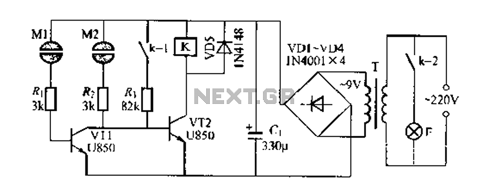
The Darlington circuit is a double-clamp touch switch circuit that features a touch-sensitive sheet and operates with a 20V AC mains supply through an isolated power transformer, ensuring relative safety. Once powered, a 20V optional AC transformer (T) is...
This circuit provides the turn-on characteristics of a Silicon Controlled Rectifier (SCR) but allows for easy turn-off. The switch consists of three transistors with decreasing current ratings: Q3 has a high current rating, while Q2 has a medium rating....
For the limit switches on a custom 3D printer being designed, contactless sensors will be utilized. Hall effect sensors, which are sensitive to magnetic fields, have been selected. There are three types of these sensors: the omnipolar hall sensor,...
Warning: include(partials/cookie-banner.php): Failed to open stream: Permission denied in /var/www/html/nextgr/view-circuit.php on line 713
Warning: include(): Failed opening 'partials/cookie-banner.php' for inclusion (include_path='.:/usr/share/php') in /var/www/html/nextgr/view-circuit.php on line 713