Transimpedance Amplifier Design
1. Definition and Basic Operation
Definition and Basic Operation
A transimpedance amplifier (TIA) is a current-to-voltage converter widely used in applications where low-level current signals from photodiodes, sensors, or other high-impedance sources must be amplified and converted into a measurable voltage. The fundamental operation relies on an operational amplifier (op-amp) with a feedback resistor, which sets the gain and ensures stability.
Core Principle
The TIA’s operation is governed by Ohm’s Law, where the output voltage Vout is proportional to the input current Iin multiplied by the feedback resistance Rf:
The negative sign indicates phase inversion due to the op-amp’s inverting configuration. The feedback resistor Rf dominates the transimpedance gain (ZT), defined as:
Key Components
- Operational Amplifier: Provides high open-loop gain and low input bias current, critical for minimizing errors in current sensing.
- Feedback Resistor (Rf): Determines the gain and bandwidth trade-off. Higher values increase sensitivity but may reduce bandwidth.
- Feedback Capacitor (Cf): Compensates for parasitic capacitances to prevent instability or oscillation.
Stability and Bandwidth Considerations
The TIA’s bandwidth is limited by the op-amp’s gain-bandwidth product (GBWP) and the RC time constant formed by Rf and the total input capacitance (Cin). The -3 dB bandwidth is approximated as:
For stability, the feedback capacitor Cf must be chosen to ensure the phase margin exceeds 45°. A common design rule is:
Practical Applications
TIAs are indispensable in:
- Optical receivers: Converting photodiode currents to voltages in fiber-optic systems.
- Sensor interfaces: Amplifying signals from piezoelectric or electrochemical sensors.
- High-speed instrumentation: Enabling low-noise current measurements in oscilloscopes and spectrum analyzers.
1.2 Key Performance Parameters
Transimpedance Gain (ZT)
The transimpedance gain (ZT) defines the amplifier’s ability to convert input current to output voltage, expressed as:
For an ideal operational amplifier (op-amp) with feedback resistor Rf, the gain simplifies to:
Non-idealities such as finite op-amp gain and parasitic capacitances introduce deviations. In practice, ZT is frequency-dependent due to the amplifier’s bandwidth limitations and the RfCf network’s pole.
Bandwidth and Stability
The bandwidth of a transimpedance amplifier (TIA) is determined by the dominant pole formed by Rf and the total input capacitance (Cin), which includes the photodiode capacitance and amplifier input capacitance. The -3 dB bandwidth is approximated by:
Stability is governed by the phase margin of the loop gain. A common stability criterion requires the amplifier’s gain-bandwidth product (GBW) to satisfy:
where Cf is the feedback capacitance added to compensate for peaking or oscillations.
Noise Performance
The total input-referred noise current of a TIA combines contributions from:
- Thermal noise of Rf: $$ i_{n,R_f} = \sqrt{\frac{4kT}{R_f}} $$
- Op-amp voltage noise (en): $$ i_{n,op} = e_n \sqrt{\frac{1}{R_f^2} + (2\pi C_{in}f)^2} $$
- Shot noise from the photodiode dark current (Idark): $$ i_{n,shot} = \sqrt{2qI_{dark}} $$
The equivalent noise current density (in pA/√Hz) is critical for low-light applications such as LiDAR or optical communications.
Dynamic Range
The dynamic range spans from the minimum detectable current (set by noise) to the maximum linear current (limited by op-amp slew rate or Rf power dissipation). For a TIA with output swing Vmax:
High dynamic range often requires trade-offs between gain, bandwidth, and noise. For example, increasing Rf improves sensitivity but reduces bandwidth.
Input Impedance and Loading Effects
A TIA’s input impedance (Zin) must be sufficiently low to prevent signal attenuation. For an ideal op-amp:
where A(s) is the op-amp’s open-loop gain. At high frequencies, Zin increases due to gain roll-off, potentially degrading performance for high-capacitance photodiodes.
Power Supply Rejection Ratio (PSRR)
PSRR quantifies the amplifier’s immunity to power supply variations. For TIAs, poor PSRR can couple supply noise directly into the output. A typical specification might require:
Low-noise designs often employ regulated supplies or differential topologies to mitigate this effect.
Temperature Drift
Key parameters such as Rf tolerance and op-amp offset voltage vary with temperature. The drift in transimpedance gain is given by:
where αRf is the resistor’s temperature coefficient and ΔVos is the offset drift. Precision applications use low-drift components or active compensation techniques.
1.3 Applications in Modern Electronics
Transimpedance amplifiers (TIAs) serve as critical building blocks in numerous high-performance electronic systems where current-to-voltage conversion with low noise and wide bandwidth is essential. Their unique ability to amplify weak photocurrents while maintaining signal integrity makes them indispensable in several cutting-edge applications.
Optical Communication Systems
In fiber-optic networks, TIAs form the front-end of optical receivers, converting photodiode-generated currents into usable voltage signals. The transimpedance gain ZT must be carefully optimized to balance sensitivity and bandwidth:
where Rf is the feedback resistor and Cf represents the total parasitic capacitance. Modern 400G coherent receivers employ differential TIAs with >50 GHz bandwidth, requiring careful stability analysis via the Barkhausen criterion.
Biomedical Instrumentation
TIAs enable precise measurement of biopotentials in:
- Pulse oximeters (photoplethysmography)
- DNA sequencers (fluorescence detection)
- Neural recording systems (microelectrode arrays)
For example, in confocal microscopy, the TIA's input-referred current noise in directly impacts detection limits:
Quantum Sensing Applications
Single-photon avalanche diode (SPAD) arrays in quantum key distribution systems require TIAs with sub-nA resolution. The equivalent noise charge (ENC) becomes the limiting factor:
where T is the integration time and Ctot includes photodiode and amplifier capacitances. Cryogenic TIAs for superconducting nanowire detectors push this further, achieving <100 pA/√Hz noise floors.
Industrial Sensing Systems
LIDAR systems for autonomous vehicles use multi-channel TIAs with:
- Time-gain compensation for varying target distances
- Adaptive bandwidth control to reject ambient light
- Integrated analog-to-digital conversion
The signal-to-noise ratio (SNR) in such pulsed systems depends critically on the TIA's rise time tr:
where Cd is the detector capacitance and Cin the amplifier input capacitance. Modern integrated TIAs achieve <500 ps rise times through heterojunction bipolar transistor (HBT) processes.
2. Op-Amp Selection Criteria
2.1 Op-Amp Selection Criteria
Key Parameters for Transimpedance Amplifiers
The operational amplifier (op-amp) is the core component of a transimpedance amplifier (TIA), and its selection critically impacts performance. The following parameters must be evaluated:
- Input Bias Current (Ib) – Must be minimized to avoid introducing errors in low-current applications. FET-input op-amps (e.g., JFET or CMOS) are preferred for photodiode applications.
- Input Voltage Noise (en) – Dominates noise performance at higher frequencies. A lower en is crucial for high-speed or low-light applications.
- Gain-Bandwidth Product (GBW) – Determines the amplifier's frequency response. Must exceed the desired bandwidth by a sufficient margin.
- Slew Rate (SR) – Affects the amplifier's ability to respond to fast current transients without distortion.
Noise Considerations
The total noise in a TIA is a combination of:
- Current Noise (in) – Primarily relevant for high-source-impedance applications.
- Thermal Noise from Feedback Resistor (Rf) – Given by:
where k is Boltzmann's constant, T is temperature, and Δf is the bandwidth.
The op-amp's voltage noise contribution is amplified by the noise gain, which for a TIA is:
where Cd is the photodiode capacitance, Cin is the op-amp input capacitance, and Cf is the feedback capacitance.
Stability and Compensation
Phase margin must be carefully evaluated to prevent oscillations. The dominant pole is set by:
Adding a feedback capacitor Cf helps stabilize the amplifier by introducing a zero:
For stability, the op-amp's GBW should satisfy:
Practical Op-Amp Selection
For high-performance TIAs, consider the following op-amps:
- Low-Noise, Low-Ib Op-Amps: OPA828, LTC6268 (for precision applications).
- High-Speed Op-Amps: OPA657, ADA4817 (for bandwidths >100 MHz).
- Low-Power Op-Amps: AD8615, MAX44260 (for portable or battery-operated systems).
Trade-offs between bandwidth, noise, and power consumption must be carefully balanced based on application requirements.
2.2 Feedback Resistor Design
Key Role of the Feedback Resistor
The feedback resistor Rf in a transimpedance amplifier (TIA) determines the gain-bandwidth trade-off and noise performance. The transimpedance gain ZT is given by:
For a photodiode with current Iph, the output voltage scales linearly with Rf. However, increasing Rf also amplifies thermal noise, given by:
Stability and Bandwidth Considerations
The feedback resistor interacts with the photodiode capacitance Cd and amplifier input capacitance Cin, forming a pole that limits bandwidth:
To ensure stability, the phase margin must be sufficient. A common design rule restricts the gain-bandwidth product (GBW) of the op-amp:
Noise Optimization
The total input-referred noise current combines resistor thermal noise and amplifier voltage noise:
For low-noise designs, Rf should be large enough to dominate amplifier noise but not so large that bandwidth is excessively reduced.
Practical Selection Guidelines
- High-speed applications: Use lower Rf (100Ω–10kΩ) with wideband amplifiers.
- Precision measurements: Higher Rf (1MΩ–1GΩ) with low-noise op-amps.
- Trade-off: Parallel resistors or T-networks can extend dynamic range.
Parasitic Effects
At high frequencies, parasitic inductance and capacitance of Rf become significant. Surface-mount resistors with minimal lead length are preferred for GHz operation.
2.3 Stability and Compensation Techniques
Transimpedance amplifiers (TIAs) are prone to instability due to the interaction between the feedback resistor Rf and the photodiode capacitance Cd. The feedback network introduces a pole that, when combined with the amplifier's intrinsic poles, can lead to peaking or even oscillation. Stability analysis requires evaluating the loop gain and phase margin.
Loop Gain and Phase Margin
The loop gain T(s) of a TIA is given by:
where A(s) is the open-loop gain of the amplifier. The dominant pole ωp arises from the feedback network:
Phase margin (PM) is a critical metric for stability. A PM > 45° is typically required to avoid excessive peaking, while PM > 60° ensures a well-damped response. The phase margin can be approximated as:
where ωu is the unity-gain frequency of the amplifier.
Compensation Techniques
To improve stability, several compensation techniques are employed:
1. Feedback Capacitance (Cf)
Adding a small capacitor Cf in parallel with Rf introduces a zero that counters the phase lag:
The optimal value of Cf is determined by:
2. Noise Gain Compensation
By intentionally increasing the noise gain at high frequencies, the amplifier's bandwidth is reduced, improving phase margin. This is achieved by adding a capacitor Cn from the inverting input to ground:
3. Dominant Pole Compensation
Introducing a low-frequency pole inside the amplifier (e.g., by increasing the compensation capacitor) reduces the bandwidth but enhances stability. The modified dominant pole becomes:
Practical Considerations
In high-speed TIAs, parasitic capacitances from PCB traces and packaging must be minimized. A well-designed layout reduces stray capacitance at the inverting input, which otherwise degrades stability. Additionally, selecting an amplifier with sufficiently low input capacitance is crucial.
Simulation tools like SPICE are indispensable for verifying stability. A Bode plot of the loop gain reveals the phase margin, while transient analysis checks for ringing or oscillation.
2.4 Noise Analysis and Mitigation
Noise Sources in Transimpedance Amplifiers
The dominant noise sources in a transimpedance amplifier (TIA) include:
- Photodiode shot noise - Arises from the statistical nature of photon-to-electron conversion.
- Johnson-Nyquist noise - Thermal noise from the feedback resistor.
- Amplifier voltage noise - Input-referred noise of the op-amp.
- Amplifier current noise - Input bias current fluctuations.
The total input-referred noise current spectral density is given by:
where q is the electron charge, Ip is the photocurrent, k is Boltzmann's constant, T is temperature, Rf is the feedback resistance, and Ctotal is the sum of photodiode and amplifier input capacitances.
Noise Optimization Techniques
Feedback Resistor Selection
The feedback resistor value presents a trade-off between bandwidth and noise:
where f-3dB is the desired bandwidth. While larger Rf reduces thermal noise, it also limits bandwidth. For ultra-low noise applications, consider:
- Cryogenic cooling to reduce thermal noise
- Using a T-network to achieve high effective resistance while maintaining bandwidth
Amplifier Selection Criteria
Choose operational amplifiers with:
- Ultra-low input current noise (<0.1 fA/√Hz for precision applications)
- Low voltage noise (<1 nV/√Hz)
- High gain-bandwidth product to maintain stability with large feedback resistors
The amplifier's noise contribution becomes significant when:
Capacitance Minimization
Total input capacitance Ctotal affects both bandwidth and noise performance:
Minimization strategies include:
- Selecting photodiodes with low junction capacitance
- Using amplifiers with low input capacitance
- Careful PCB layout to minimize stray capacitance
- Guarding techniques to reduce effective input capacitance
Noise Filtering Approaches
Post-amplification filtering can improve SNR while maintaining signal integrity:
- Active filtering: Multi-pole Butterworth or Bessel filters provide steep roll-off
- Digital filtering: FIR or IIR filters in subsequent signal processing stages
- Adaptive filtering: LMS algorithms for dynamic noise environments
The optimal filter cutoff frequency balances noise reduction with signal distortion:
where tr is the signal rise time.
Practical Noise Measurement
For empirical noise characterization:
- Measure output noise spectrum with input terminated
- Subtract amplifier noise contribution through independent characterization
- Account for measurement system noise floor
- Verify results against theoretical calculations
Advanced techniques include cross-correlation measurements to reject uncorrelated noise from the measurement system.
3. PCB Layout Best Practices
3.1 PCB Layout Best Practices
Transimpedance amplifier (TIA) performance is highly sensitive to parasitic capacitances, ground loops, and electromagnetic interference (EMI). A well-optimized PCB layout minimizes these effects while maintaining signal integrity. Key considerations include component placement, grounding strategies, and trace routing.
Component Placement
The photodiode should be placed as close as possible to the TIA input to minimize parasitic capacitance (Cp). For a feedback resistor Rf and input capacitance Cin, the bandwidth is given by:
Parasitic capacitance from long traces can dominate Cin, reducing bandwidth. Place critical components (photodiode, TIA, feedback network) in a compact, shielded region.
Grounding and Shielding
Use a star-ground configuration with separate analog and digital ground planes, connected at a single point near the power supply. The TIA ground return path must have low impedance to prevent ground-induced noise. For high-gain designs (>1 MΩ), guard rings around sensitive nodes reduce leakage currents:
- Route guard traces at the same potential as the guarded node (e.g., TIA output for feedback traces)
- Use via stitching to create a Faraday cage around high-impedance paths
- Implement split ground planes only when necessary, as improper use increases EMI susceptibility
Trace Routing and Layer Stackup
High-speed TIAs require controlled impedance traces. For a microstrip trace over a ground plane, characteristic impedance (Z0) is:
where h is dielectric thickness, w is trace width, t is trace thickness, and ϵr is substrate permittivity. Best practices include:
- Keep input traces shorter than λ/10 at the highest frequency of interest
- Use 45° miters instead of 90° bends to reduce reflections
- Route sensitive traces on inner layers between ground planes for shielding
Power Supply Decoupling
Place decoupling capacitors (typically 100 nF ceramic + 10 μF tantalum) within 5 mm of the TIA power pins. The capacitor's effective series inductance (ESL) forms a resonant circuit:
Multi-stage decoupling with different capacitor values suppresses resonance effects. Place smaller capacitors closer to the IC.
Thermal Management
Power dissipation in the feedback resistor (P = Ipd2Rf) can cause thermal drift. Use:
- Thermal relief pads for through-hole components
- Copper pours connected to ground planes as heat sinks
- Temperature-stable resistors (e.g., metal foil) for precision applications
3.2 Thermal Management
Thermal Noise and Its Impact on Performance
Thermal noise, or Johnson-Nyquist noise, arises due to the random motion of charge carriers in resistive elements. In a transimpedance amplifier (TIA), this manifests as voltage fluctuations at the input, degrading the signal-to-noise ratio (SNR). The thermal noise voltage spectral density is given by:
where k is Boltzmann's constant (1.38 × 10⁻²³ J/K), T is the absolute temperature in Kelvin, and R is the feedback resistance. Excessive heat increases T, raising noise and introducing drift in component parameters.
Power Dissipation in Feedback Components
The feedback resistor (Rf) dissipates power proportional to the square of the input current:
High-gain TIAs with large Rf (e.g., 1 MΩ to 1 GΩ) are particularly susceptible. For example, a 1 μA input current through a 1 MΩ resistor dissipates 1 μW, while 10 μA dissipates 100 μW—enough to cause measurable temperature rise in precision circuits.
Thermal Resistance and Junction Temperature
The operational amplifier's junction temperature depends on the thermal resistance (θJA) and ambient conditions:
where TA is ambient temperature, and PD is the total power dissipated by the op-amp. For a typical SOIC-8 package, θJA ≈ 160°C/W. A 50 mW dissipation raises the junction temperature by 8°C above ambient, potentially altering bias currents and offset voltages.
Mitigation Strategies
1. Material Selection
- Low-TCR resistors: Metal-film or bulk-metal resistors (TCR < 10 ppm/°C) minimize resistance drift.
- Thermally stable op-amps: Chopper-stabilized amplifiers (e.g., LTC2050) reduce offset drift to < 0.05 μV/°C.
2. Layout Techniques
- Thermal reliefs: Use star grounding and thermal pads to distribute heat away from sensitive nodes.
- Copper pours: Increase PCB copper area around high-power components to lower θJA.
3. Active Cooling
For high-power designs (>100 mW), forced-air cooling or Peltier elements stabilize temperature. A case study in LIDAR systems showed a 20°C reduction in TJ using a 4 cm2 heatsink, improving SNR by 3 dB.
Thermal Simulation and Validation
Finite-element analysis (FEA) tools like ANSYS Icepak predict thermal gradients. A validated model for a 10 GΩ TIA showed a 5°C hotspot at Rf, correlating with a 0.1% gain error. Infrared thermography is recommended for experimental validation.
where α is the resistor's temperature coefficient. For a 100 ppm/°C resistor, a 10°C rise induces a 0.1% error—critical in photodiode applications requiring < 0.01% stability.
3.3 Shielding and EMI Reduction
Electromagnetic Interference (EMI) Mechanisms
EMI in transimpedance amplifiers (TIAs) arises from capacitive/inductive coupling of external noise sources into high-impedance nodes. The input current-to-voltage conversion stage is particularly vulnerable due to its high gain at low frequencies. Radiated EMI couples through parasitic capacitances (Cp), while conducted EMI enters via power supply lines or ground loops. For a TIA with feedback resistance Rf, the induced noise voltage Vn due to EMI current Iemi is:
Shielding Strategies
Faraday cages around sensitive components attenuate radiated EMI by reflecting/absorbing electromagnetic waves. For optimal performance:
- Use conductive enclosures with seams shorter than λ/20 at the highest frequency of concern
- Ground shields at a single point to avoid ground loops
- Select materials based on skin depth: copper (≥1 MHz), mu-metal (≤100 kHz)
The shielding effectiveness (SE) in dB for a solid shield is:
where A is absorption loss, R reflection loss, and K multiple-reflection correction.
PCB Layout Techniques
Critical layout practices for EMI suppression:
- Guard rings: Surround high-impedance traces with grounded copper to shunt leakage currents
- Differential routing: Route photodiode connections as twisted pairs or microstrip lines
- Ground planes: Use multilayer PCBs with dedicated ground layers (≥4 layers recommended)
The parasitic capacitance Cp between adjacent traces spaced by d is:
where w is trace width and l parallel length.
Filtering Methods
Combine passive and active filtering:
- Input RC filters: Place series resistors (10–100Ω) and parallel capacitors (100 pF–1 nF) at the TIA input
- Power supply decoupling: Use parallel 100 nF (ceramic) and 10 μF (tantalum) capacitors
- Feedforward compensation: Add a capacitor across feedback resistor to limit bandwidth
The −3dB cutoff frequency for an input RC filter is:
Component Selection
Choose components with low EMI susceptibility:
- Photodiodes: Select devices with small junction capacitance (<1 pF for high-speed apps)
- Op-amps: Use current-feedback amplifiers (CFAs) for GHz-range TIAs
- Resistors: Metal-film types exhibit lower parasitic inductance than carbon composition
4. High-Speed Transimpedance Amplifiers
4.1 High-Speed Transimpedance Amplifiers
Bandwidth Limitations and Compensation Techniques
The bandwidth of a transimpedance amplifier (TIA) is fundamentally limited by the feedback resistor Rf and the total input capacitance Cin, which includes the photodiode capacitance and amplifier input capacitance. The dominant pole frequency is given by:
For high-speed applications, this bandwidth constraint becomes critical. To extend bandwidth, designers employ compensation techniques such as:
- Pole-Zero Cancellation: Introducing a compensation capacitor Cf in parallel with Rf creates a zero that counters the input pole.
- Active Feedback: Using an inductor or a capacitive peaking network to shape the frequency response.
- Noise Optimization: Balancing thermal noise (4kTRf) and bandwidth by selecting an optimal Rf.
Stability Analysis and Phase Margin
High-speed TIAs risk instability due to parasitic phase shifts. The loop gain T(s) must satisfy the Barkhausen criterion for stability. The phase margin (PM) is derived from the open-loop transfer function:
where AOL(s) is the open-loop gain and β(s) is the feedback factor. For stability, PM should exceed 45°–60°. A practical approach involves:
- Dominant Pole Compensation: Adjusting Cf to ensure the secondary poles are beyond the unity-gain frequency.
- Transient Analysis: Simulating step responses to verify overshoot and ringing.
Noise Considerations in High-Speed Designs
In high-speed TIAs, noise performance is dominated by:
where in,amp is the amplifier’s input-referred noise current. Key noise-reduction strategies include:
- Low-Noise Op-Amps: Selecting amplifiers with sub-pA/√Hz noise density.
- Capacitive Matching: Minimizing Cin to reduce the noise gain peaking effect.
Case Study: 10 Gbps Optical Receiver
A 10 Gbps TIA for fiber-optic systems exemplifies these principles. Key parameters:
- Bandwidth: ≥7 GHz to accommodate NRZ modulation.
- Transimpedance Gain: 1 kΩ–5 kΩ, balancing sensitivity and speed.
- Noise: <3 pA/√Hz to maintain a 10−12 BER.
Such designs often employ InGaAs photodiodes (Cpd ≈ 0.2 pF) and SiGe or CMOS amplifiers with fT > 50 GHz.
4.2 Low-Noise Design Techniques
Noise Sources in Transimpedance Amplifiers
The dominant noise sources in a transimpedance amplifier (TIA) include:
- Johnson-Nyquist (thermal) noise from the feedback resistor \(R_f\).
- Shot noise from the photodiode dark current and signal current.
- Op-amp voltage and current noise, including \(1/f\) (flicker) noise.
The total input-referred noise current spectral density \(i_{n,\text{total}}\) is given by:
Minimizing Thermal Noise
Thermal noise from \(R_f\) is governed by \(4kT/R_f\). To reduce it:
- Maximize \(R_f\) while maintaining bandwidth requirements.
- Use low-temperature-coefficient resistors (e.g., metal foil) to avoid drift.
The bandwidth constraint imposes an upper limit on \(R_f\):
where \(C_{\text{total}}\) is the sum of photodiode capacitance \(C_d\) and op-amp input capacitance \(C_{\text{in}}\).
Op-Amp Selection Criteria
Choose an op-amp with:
- Ultra-low input current noise (\(i_n < 1 \text{pA}/\sqrt{\text{Hz}}\)).
- Low voltage noise (\(v_n < 3 \text{nV}/\sqrt{\text{Hz}}\)).
- High gain-bandwidth product to avoid bandwidth penalties.
The noise contribution from the op-amp becomes significant when:
Capacitance Management
Stray capacitances exacerbate noise by reducing the effective feedback impedance. Mitigation strategies include:
- Minimizing PCB trace lengths to reduce parasitic capacitance.
- Using guard rings to shield high-impedance nodes.
- Selecting photodiodes with low junction capacitance (\(C_d\)).
Active Noise Cancellation Techniques
Advanced designs may incorporate:
- Bootstrapping to reduce effective \(C_d\).
- Noise-canceling architectures using auxiliary amplifiers.
- Chopper stabilization to mitigate \(1/f\) noise.
The effectiveness of noise cancellation is quantified by the improvement in signal-to-noise ratio (SNR):
Practical Implementation Example
For a 100 MHz bandwidth TIA with a InGaAs photodiode (\(C_d = 5 \text{pF}\)):
- Selected \(R_f = 1 \text{k}\Omega\) yields \(f_{\text{BW}} = 31.8 \text{MHz}\) before compensation.
- Added \(C_f = 0.5 \text{pF}\) for peaking control, achieving flat response.
- Used an OPA657 op-amp (\(v_n = 4.3 \text{nV}/\sqrt{\text{Hz}}\), \(i_n = 1.3 \text{fA}/\sqrt{\text{Hz}}\)) for optimal noise performance.
4.3 Bandwidth Extension Methods
The bandwidth of a transimpedance amplifier (TIA) is fundamentally limited by the interaction between the feedback resistor Rf and the total input capacitance Cin, which includes the photodiode capacitance and amplifier input capacitance. The dominant pole frequency is given by:
For high-speed applications, this bandwidth is often insufficient. Several techniques exist to extend the bandwidth while maintaining stability and noise performance.
1. Capacitive Peaking
Adding a small capacitor Cf in parallel with Rf creates a zero in the transfer function that can partially compensate the dominant pole. The modified transfer function becomes:
The optimal value for Cf is typically 10-30% of Cin. While this method provides modest bandwidth improvement, excessive peaking can lead to instability.
2. Inductive Peaking
Placing a small inductor in series with Rf introduces a complex pole pair that can extend bandwidth. The inductor value is chosen to resonate with the total input capacitance:
This technique is particularly effective in multi-gigahertz applications, though it requires careful PCB layout to minimize parasitic effects.
3. Active Feedback
Replacing the passive feedback network with an active circuit can significantly improve bandwidth. One common approach uses a common-gate (or common-base) stage:
where gm is the transconductance of the active device. This reduces the effective feedback impedance at high frequencies while maintaining DC gain.
4. Current-Mode Feedback
Current-mode feedback techniques use a current mirror to sense the photodiode current and feed it back directly, avoiding the bandwidth limitation of voltage feedback. The bandwidth becomes primarily limited by the transistor fT rather than the RC time constant.
5. Distributed Amplification
For extremely wideband applications, distributed amplifiers employ multiple gain stages with artificial transmission lines to achieve bandwidths exceeding 100 GHz. The effective input capacitance is divided among several stages:
where N is the number of stages. This approach is commonly used in optical communication receivers.
Practical Considerations
When implementing bandwidth extension techniques, several tradeoffs must be considered:
- Noise performance: Active techniques typically increase noise
- Power consumption: More complex circuits require higher power
- Stability: Additional poles and zeros must be carefully compensated
- Linearity: Some methods introduce nonlinear distortion
The choice of method depends on the specific application requirements for bandwidth, noise, and power. In practice, a combination of techniques is often employed to achieve optimal performance.
5. Key Research Papers
5.1 Key Research Papers
- Analysis and design of transimpedance amplifiers for optical receivers — 1 Introduction 1 1.1 Optical Transceivers 1 1.2 Modulation Formats 5 1.3 Transmission Modes 12 References 20 ... 6 Basic Transimpedance Amplifier Design 201 6.1 Low and High Impedance Front Ends 202 6.2 Shunt Feedback TIA 205 6.3 Noise Analysis 224 6.4 Noise Optimization 236 6.5 Noise Matching 248 6.6 Summary 260 Problems 262 References 265 ...
- PDF Design on Transimpedance Amplifier for Optical Communications — bias current to prevent the front-end transimpedance ampli er from saturation. The allowed input current range, because of this design, is from 10 A to 1 mA: The designed transimpedance IC, after the post-simulation, attains the transimpedance gain 63 dB, the bandwidth 4.5 GHz, and the input referred noise 1.1 A; and is well suitable for
- (PDF) Design of a CMOS Broadband Transimpedance Amplifier With Active ... — This is implemented in 32 nm CMOS technology using Custom Designer from Synopsys. The circuit is designed to compete with existing transimpedance amplifiers implemented in other technologies in the field of optical communications. The transimpedance amplifier design in this study has a gain of 54 dB and a bandwidth of 9.39 GHz.
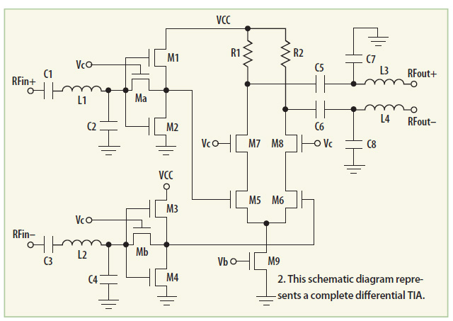
- PDF DESIGN OF A LOW POWER 5-Gb/s FULLY BALANCED AND DIFFERENTIAL OUTPUT ... — Figure 4.1 Proposed Block Diagram of Differential TIA Design 64 Figure 4.2 Small Signal Analysis of Differential TIA Design 68 Figure 4.3 Layout of RGC Design 73 Figure 4.4 Layout of Source-Degenerated Differential Ampliï¬er Design 75 Figure 4.5 Layout of Folded-Cascode Opamp 76 Figure 4.6 Layout of Output Buffer Design 77
- PDF AN-1803 Design Considerations for a Transimpedance Amplifier — light. The transimpedance amplifier (TIA) is utilized to convert this low-levelcurrent to a usable voltage signal and the TIA often needs to be compensated for proper operation. This application report explores a simple TIA design using a 345 MHz rail-to-railoutput VFA, such as TI's LMH6611. The main goal of this
- Design of Differential Variable-Gain Transimpedance Amplifier in ... - MDPI — This paper presents two new inductorless differential variable-gain transimpedance amplifiers (DVGTIA) with voltage bias controlled variable gain designed in TowerJazz's 0.18 µm SiGe BiCMOS technology (using CMOS transistors only). Both consist of a modified differential cross-coupled regulated cascode preamplifier stage and a cascaded amplifier stage with bias-controlled gain-variation and ...
- PDF CHAPTER 6 Transimpedance Amplifier Design - Springer — amplifier configuration for frequency-domain analysis, where i PD is the photocurrent generator from optoelectronic conversion of the incoming light and C f a shunt feedback capacitor. FIGURE 6.3. Transimpedance amplifier configuration BW 1 2SR TIAC PD-----major limitation of this structure. Design for high gain in the passive stage leads to a ...
- PDF Design of A 20mhz Transimpedance Amplifier With Embedded Low-pass ... — DESIGN OF A 20MHZ TRANSIMPEDANCE AMPLIFIER . WITH EMBEDDED LOW-PASS FILTER . FOR A DIRECT CONVERSION WIRELESS RECEIVER . A Thesis . by . CHARLES PROF SEKYIAMAH . Submitted to the Office of Graduate Studies of . Texas A&M University . in partial fulfillment of the requirements for the degree of . MASTER OF SCIENCE . August 2011 . Major Subject ...
- PDF Analysis and Design of Wideband CMOS Transimpedance Amplifiers Using ... — Analysis and Design of Wideband CMOS Transimpedance Amplifiers Using Inductive Feedback Omidreza Ghasemi, Ph.D. Concordia University, 2012 Optical receivers have an important role in high data rate wireline data communication systems. Nowadays, these receivers have data rates of multi Gb/s. To achieve such high data rate in the
5.2 Recommended Textbooks
- Analysis and design of transimpedance amplifiers for optical receivers — Stanford Libraries' official online search tool for books, media, journals, databases, ... 6 Basic Transimpedance Amplifier Design 201; 6.1 Low and High Impedance Front Ends 202; 6.2 Shunt Feedback TIA 205; ... (electronic bk.) 9781119264415 (electronic bk.) 1119264413 (electronic bk.) 9781119263777
- Photodetectors: Devices, Circuits and Applications: Front Matter — 5.3.2.1 High-Frequency Transimpedance Amplifiers (TIA) 160 5.3.2.2 Equalization Technique 165 5.3.2.3 Switched Capacitor Technique 168 References 172 Problems173 Chapter 6 Avalanche Photodiode, SPAD and SiPM 175 6.1 Avalanche Photodiode 175 6.1.1 Gain of the APDs 177 6.1.2 Frequency Response and Noise 180
- Reference Design for Extending OPA857 Transimpedance Bandwidth — Reference Design for Extending OPA857 Transimpedance Bandwidth 4 System Design Theory An op-amp with wide bandwidth is the core of the TIA block of the OPA857, shown in Figure 2. The CTRL logic controls an internal single-pole double throw (SPDT) switch to configure the amplifier in a transimpedance gain of 5 kΩor 20 kΩ.
- PDF Build a Programmable Gain Transimpedance Amplifier Using the OPA3S328 — Build a Programmable Gain Transimpedance Amplifier Using the OPA3S328 Luis Chioye ABSTRACT The OPA3S328 is a 40-MHz, dual, precision, low input bias current, CMOS operational amplifier (op-amp) with integrated switches optimized for programmable gain transimpedance amplifier applications. The device offers a
- PDF High Performance Design Techniques of Transimpedance Amplifier — transimpedance amplifier for over new technologies by using cross coupled current conveyor stage with input have series inductive peaking and output provided with capacitive degeneration stage; this procedure provides larger improvements over traditional designs of transimpedance amplifier. 4. REFERENCES transimpedance amplifier".
- PDF Design on Transimpedance Amplifier for Optical Communications — bias current to prevent the front-end transimpedance ampli er from saturation. The allowed input current range, because of this design, is from 10 A to 1 mA: The designed transimpedance IC, after the post-simulation, attains the transimpedance gain 63 dB, the bandwidth 4.5 GHz, and the input referred noise 1.1 A; and is well suitable for
- PDF Design of A 20mhz Transimpedance Amplifier With Embedded Low-pass ... — DESIGN OF A 20MHZ TRANSIMPEDANCE AMPLIFIER . WITH EMBEDDED LOW-PASS FILTER . FOR A DIRECT CONVERSION WIRELESS RECEIVER . A Thesis . by . CHARLES PROF SEKYIAMAH . Submitted to the Office of Graduate Studies of . Texas A&M University . in partial fulfillment of the requirements for the degree of . MASTER OF SCIENCE . August 2011 . Major Subject ...
- Analysis and Design of Transimpedance Amplifiers for Optical Receivers — Analysis and Design of Transimpedance Amplifiers for OpticalReceivers belongs on the reference shelves of every electrical engineer working in the IC and optical industries. It also can serve as a textbook for upper-level undergraduates and graduate students studying integrated circuit design and optical communication.
- Analysis and design of transimpedance amplifiers for... — Read online or download for free from Z-Library the Book: Analysis and design of transimpedance amplifiers for optical receivers, Author: Säckinger, Eduard ...
- Table of Contents - The Art of Electronics 3rd Edition — FOUR: Operational Amplifiers. 4.1 Introduction to op-amps - the "perfect component" 4.2 Basic op-amp circuits 4.3 An op-amp smorgasbord 4.4 A detailed look at op-amp behavior 4.5 A detailed look at selected op-amp cir- cuits 4.6 Op-amp operation with a single power supply 4.7 Other amplifiers and op-amp types 4.8 Some typical op-amp circuits
5.3 Online Resources and Tools
- High-Speed, Linear Transimpedance Amplifier Reference Design — Resources TIDA-01350 Design Folder LMH5401 Product Folder TINA-TI™ Tools Folder ASK Our E2E Experts ... Linear Transimpedance Amplifier Reference Design 1 System Description The TIDA-01350 TI Design is a fixed-gain, high-bandwidth, fully-differential, current-to-voltage conversion ... (1 / 0.5) = 3.0 dB. A fully-modulated signal where the ...
- Analysis and Design of Transimpedance Amplifiers for Optical Receivers — chapter 6: Basic Transimpedance Amplifier Design. 6.1 Low- and High-Impedance Front-Ends; 6.2 Shunt-Feedback TIA; 6.3 Noise Analysis; 6.4 Noise Optimization; 6.5 Noise Matching; 6.6 Summary; Problems; References; Chapter 7: Advanced Transimpedance Amplifier Design I. 7.1 TIA with Post Amplifier; 7.2 TIA with Differential Inputs and Outputs; 7.3 ...
- Analysis and design of transimpedance amplifiers for optical receivers — Stanford Libraries' official online search tool for books, media ... 7 Advanced Transimpedance Amplifier Design I 271 7.1 TIA with Post Amplifier 271 7.2 TIA with Differential Inputs and Outputs 276 7.3 TIA with DC Input Current Control 281 7.4 TIA with Adaptive Transimpedance 284 7.5 Common Base and Common Gate TIAs 292 7.6 Regulated Cascode ...
- Broad-Band Design Techniques for Transimpedance Amplifiers — In this paper, a novel bandwidth enhancement technique based on the combination of capacitive degeneration, broad-band matching network, and the regulated cascode (RGC) input stage is proposed and analyzed, which turns the transimpedance amplifier (TIA) design into a fifth-order low-pass filter with Butterworth response. This broad-band design methodology for TIAs is presented with an example ...
- Basic Transimpedance Amplifier Design - Wiley Online Library — This chapter explores transimpedance amplifier (TIA) topologies with the low- and high-impedance front-ends. These simple front-ends illustrate important design trade-offs and motivate the need for more sophisticated TIA topologies. It analyzes the stability and the transimpedance limit of single- and multistage implementations.
- Design and analysis of CMOS RCG transimpedance amplifier based on ... — Design and analysis of CMOS RCG transimpedance amplifier based on elliptic filter approach ISSN 1751-858X Received on 25th October 2017 Revised 29th January 2018 Accepted on 14th February 2018 E-First on 25th April 2018 doi: 10.1049/iet-cds.2017.0449 www.ietdl.org Sonia Salhi1, Abdelhalim Slimane2, Hammoudi Escid1, Sid Ahmed Tedjini2
- Transimpedance amplifiers with 133 GHz bandwidth on 130 nm indium ... — This work presents two transimpedance amplifier (TIA) circuits, which when integrated with a photodiode, can operate as front-ends of OI receiver systems. In such systems, bandwidth is mainly limited by the optoelectronic transceiver components, namely the transmitter vertical-cavity surface-emitting laser (VCSEL) diodes [ 1 ] and the receiver ...
- Transimpedance Amplifiers - SpringerLink — The transimpedance amplifier (TIA) is the most suitable preamplifier configuration used for optical receivers . ... The calculated noise using simulations tools can be easily integrated up to practical bandwidths (not infinity). The practical integrated noise bandwidth is 1.57 times the TIA bandwidth as an upper limit for a first order (one ...
- Transimpedance Amplifier Circuit Examples - Analysis and Design of ... — This chapter examines some representative transistor-level transimpedance amplifier (TIA) circuits taken from the literature. It discusses circuits in a broad range of technologies: bipolar junction ...
- AnalysisandDesignofTransimpedance Ampliï¬ersforOpticalReceivers — vii Contents Preface xi 1 Introduction 1 1.1 OpticalTransceivers 1 1.2 ModulationFormats 5 1.3 TransmissionModes 12 References 19 2 OpticalFibers 23 2.1 ...