
triangular wave oscillator
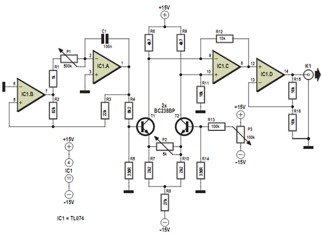
The described circuit serves as a modern alternative to the obsolete 8038 chip, focusing on the generation of sine wave signals suitable for driving LVDT sensors. The use of the TL074 operational amplifier is advantageous due to its availability and versatility. The configuration begins with two op-amps (IC1. A and B) configured as integrators to produce a triangular waveform. The frequency of this waveform is adjustable through the potentiometer P1, allowing for a range of operational frequencies based on the application requirements.
The triangular wave is then fed into a differential amplifier stage composed of transistors T1 and T2, which shapes the waveform into a sine wave. This stage is crucial for reducing the harmonic distortion inherent in triangular waveforms, thereby enhancing the signal quality for sensitive applications such as LVDT sensors. Potentiometer P2 allows for fine-tuning of this distortion, ensuring that the output waveform closely resembles a pure sine wave.
The output from this differential amplifier is processed by a third op-amp (IC1. C) configured as a difference amplifier, which effectively presents the sine wave at its output terminal. This configuration provides the necessary gain and isolation from the previous stages. Finally, the output is buffered by the last op-amp (IC1. D) to ensure that the signal can drive subsequent circuitry without loading effects. The inclusion of potentiometer P3 allows for the adjustment of any DC offset at the output, ensuring that the signal remains centered around the desired voltage level. This comprehensive approach to circuit design not only modernizes the original application but also maintains compatibility with standard components, ensuring long-term availability and support for future designs.This design resulted from the need for a partial replacement of the well-known 8038 chip, which is no longer in production and there fore hardly obtainable. An existing design for driving an LVDT sensor (Linear Variable Differential Transformer), where the 8038 was used as a variable sine wave oscillator, had to be modernised.
It may have been pos sible to replace the 8038 with an Exar 2206, except that this chip couldn`t be used with the supply voltage used. For this reason we looked for a replacement using standard components, which should always be available.
In this circuit two opamps from a TL074 (IC1. A and B) are used to generate a triangular wave, which can be set to a wide range of frequencies using P1. The following differential ampli ¬er using T1 and T2 is con ¬gured in such a way that the triangular waveform is converted into a reasonably looking sinusoidal waveform.
P2 is used to adjust the distortion to a minimum. The third opamp (IC1. C) is configured as a difference ampli ¬er, which presents the sine wave at its output. This signal is then buffered by the last opamp (IC1. D). Any offset at the output can be nulled using P3. 🔗 External reference
Related Circuits
The Oscillator Design Guide is integrated into Agilent EEsof's Advanced Design System environment, functioning as a smart library and interactive handbook for the creation of effective designs. It facilitates quick oscillator design, interactive component characterization, and provides in-depth insights...
The notch filter can be integrated into nearly any receiver to attenuate a specific frequency by more than 30 dB. This filter is particularly useful for diminishing heterodynes and whistles. A notch filter, also known as a band-stop or band-reject...
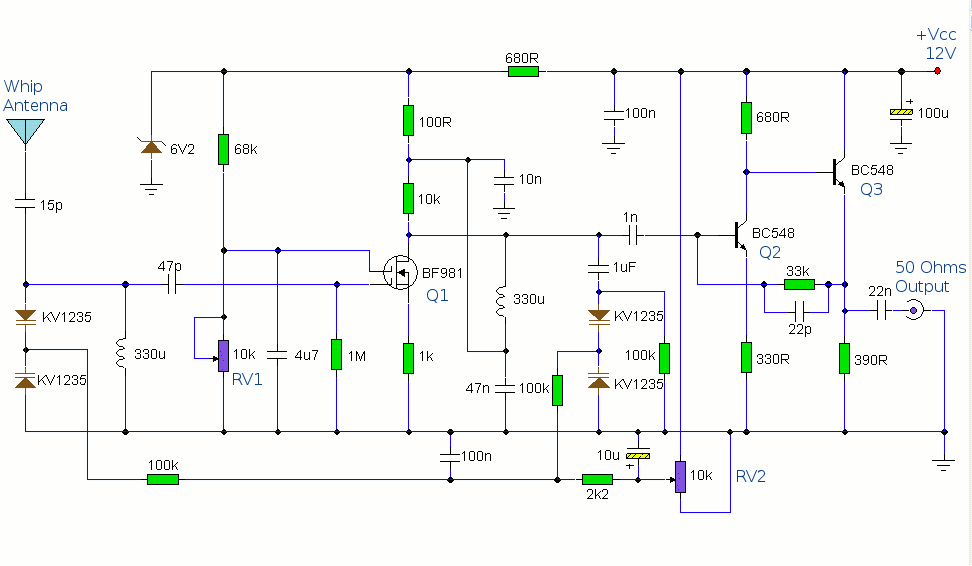
This circuit is designed to amplify the input from a telescopic whip antenna. The preamplifier is designed to cover the medium waveband from about 550KHz to 1650KHz. The tuning voltage is supplied via RV2, a 10k potentiometer connected to...

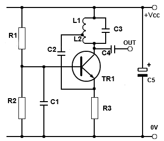
Almost any transistor will work. R1 and C1 will vary the tone. The circuit utilizes a transistor as the primary active component, which can be substituted with various types of transistors, including bipolar junction transistors (BJTs) or field-effect transistors (FETs)....
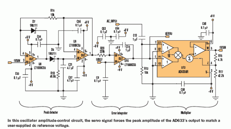
The figure illustrates a schematic for an oscillator amplitude-control servo system. The circuit establishes a closed-loop system that provides a fixed and adjustable peak-to-peak amplitude AC signal centered around 0 V. A 1 kHz sine wave, designated as AC_INPUT,...
The Hartley Oscillator is a valuable circuit for generating high-quality sine wave signals in the RF range (30 kHz to 30 MHz). However, at the upper limits of this range and beyond, the Colpitts oscillator is typically favored. Both...