
TTL oscillator
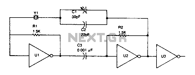
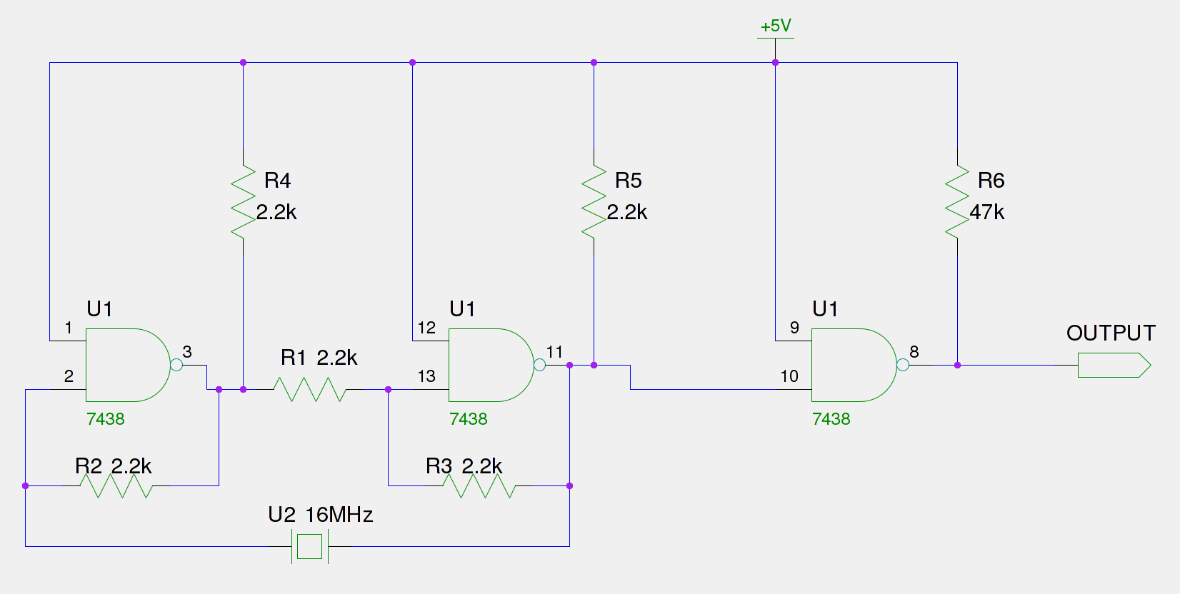
The circuit consists of two TTL inverter stages, U1 and U2, which are interconnected with a crystal oscillator component, Y1. The connection of the inverter stages through the crystal allows for the generation of a stable oscillation frequency, which is essential for various timing and clock applications in digital circuits. Each inverter stage incorporates a biasing resistor that modifies the operating point of the digital gates, enabling them to function in an analog region. This alteration allows the inverters to amplify weak signals, making them suitable for applications requiring signal conditioning.
The third inverter stage, U3, is designated as a buffer. Buffers are critical in digital circuits as they provide isolation between different circuit sections and prevent loading effects that can degrade signal integrity. The buffer stage ensures that the output from the previous stages can drive subsequent circuitry without significant signal loss or distortion. The use of a buffer also enhances the overall stability of the circuit, allowing it to maintain performance under varying load conditions.
In summary, this circuit design effectively utilizes TTL inverter stages to create a crystal-controlled oscillator while employing biasing resistors to enable amplification. The addition of a buffer stage further improves the circuit's performance by ensuring robust signal transmission. This configuration is beneficial in applications where precise timing and signal integrity are paramount.TTL inverter stages, Ul and U2, are cross-connected with a crystal Yl. A resistor in each stage biases the normally digital gates into a region where they operate as amplifiers Inverter stage U3 is used as a buffer. 🔗 External reference
Related Circuits
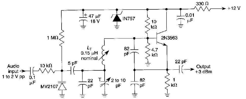
This FM oscillator can be utilized for wireless audio, microphone, and part-15 applications where a stable frequency-modulated oscillator is required. The FM oscillator is an essential component in various communication systems, particularly in wireless audio transmission and microphone applications. It...
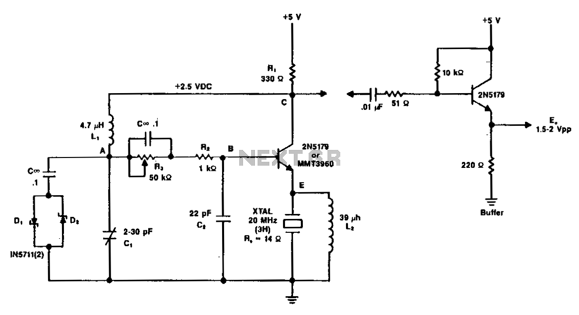
A typical circuit operating at 20 MHz is illustrated. The crystal, featuring an internal series resistance (Rs) of 14 ohms, oscillates at its third harmonic frequency. Diode clamps D1 and D2 ensure constant amplitude control. The transistor functions continuously...
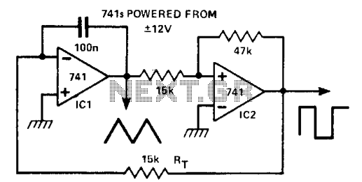
This circuit generates a triangle waveform and a square waveform simultaneously. It is self-starting and does not have latch-up issues. IC1 functions as an integrator with a slew rate determined by the capacitor (CT) and resistor (RT). IC2 acts...
Nowadays, it is no longer necessary to use discrete components to build oscillators. Instead, many manufacturers provide ready-made voltage-controlled oscillators. Modern electronic design has evolved significantly, eliminating the need for discrete components in the construction of oscillators. Voltage-controlled oscillators (VCOs)...
An old Eistar SJ-1 digital pulser has been acquired. However, the frequency it generates is consistently 66% of the expected output. The frequency observed at the frequency stage (Pin 11) is 66% of the 16 MHz crystal, which equates...
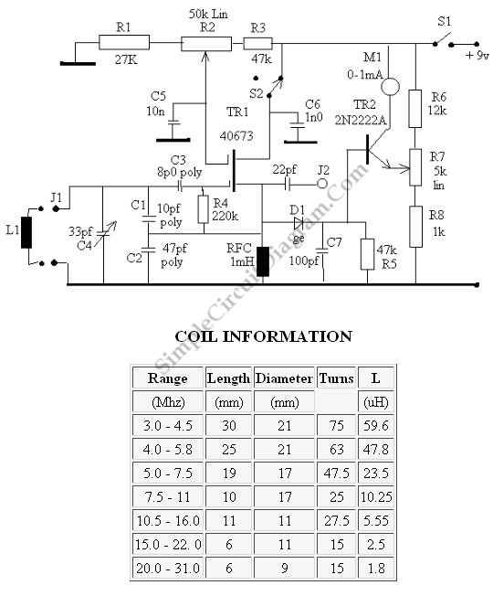
This is a grid dip oscillator (GDO) circuit developed by Luigi Falcone. The circuit uses seven plug-in coils that cover the frequency range of 3.0 to 30 MHz. It can be connected to a frequency meter through the coaxial...