
Twin-T Audio Oscillator circuit

This circuit is designed to drive a high-impedance load, which is essential for applications requiring minimal current draw from the signal source. The choice of components is critical for ensuring optimal performance. The PNP transistor option allows for versatility in circuit design, particularly in applications where a negative voltage supply is preferred. When using an op-amp, the configuration must ensure that the inverting and non-inverting inputs are correctly connected to maintain the desired feedback and gain characteristics.
The resistor values are defined with R1 and R2 being equal, which can help stabilize the gain of the circuit. The relationship between R3 and R1, where R3 is set to 0.1 times R1, suggests a feedback mechanism that will influence the overall gain. Capacitors C2 and C3 being equal ensures that the timing or filtering characteristics remain consistent, while C1 being twice the value of C2 indicates a deliberate design choice to modify frequency response or filter characteristics.
The approximate values for R4 and C4 suggest that they are used for biasing and frequency response shaping within the circuit. The choice of Q1 as an NPN audio amplifier like the BC108 indicates that the circuit is likely intended for audio applications, where low distortion and adequate gain are required. The flexibility in the supply voltage (Vcc) allows for adaptability in various circuit environments, making this design suitable for prototyping or integration into larger systems.
Overall, this circuit exemplifies a straightforward yet effective approach to signal amplification and processing, suitable for a range of electronic applications.The output of this circuit should be fed into a high-impedance load, say >100K, remembering that the impedance of C4 is around 3K. A PNP transistor can also be used, with the necessary changes to the supply voltage. An op-amp can also be used, connected as follows: Op-Amp Transistor Output Collector Inverting Input Base Non-Inverting Input Emitter
R1 = R2 R3 = 0.1 x R1 C2 = C3 C1 = 2 x C2 R4 = 3K3 (approx) C4 = 50nF (approx) Q1 = any NPN audio amplifier. e.g. BC108, etc Vcc is not critical, 6 to 12Vshould work fine. Higher or lower voltages may also work OK. 🔗 External reference
Related Circuits
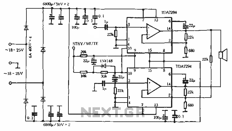
Europe's leading SGS-THOMSON STMicroelectronics recently introduced a new power integrated amplifier, the TDA7294, to the Chinese mainland market. This amplifier, characterized by a cold and hard tone, is particularly suited for Hi-Fi applications such as home theaters and active...

The circuit is designed for satellite transmission of ECG signals with a bandwidth range of 0.5 to 50 Hz, as well as other medical data within electronic systems. An audio signal serves as the FM signal source, which is...

Transistors are increasingly being utilized in various applications. Many circuits employing transistors have been developed based on previous designs that used vacuum tubes. The following chapters present unique applications that leverage the advantageous properties of transistors. The described circuits...

The tuner is programmable via I²C-Bus and provides a FBAS signal at its output. There is also the homepage of Georg Acher containing information about this tuner. A control circuit has been developed for this tuner using the AT89C2051...
This timer is designed for individuals seeking to achieve a tan while minimizing excessive exposure to sunlight. A rotary switch allows the user to set the timer based on six classified photo-types. A photoresistor adjusts the preset time value...
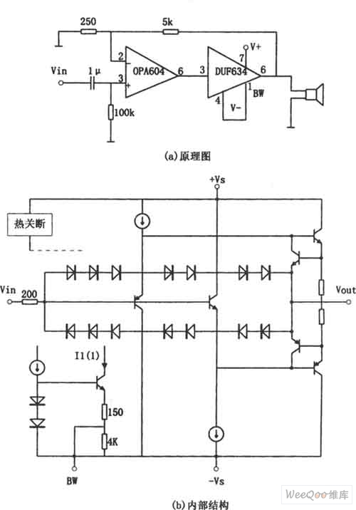
The provided image depicts a high-performance and low-power audio power amplifier circuit. The initial stage utilizes the MOSFET hi-fi operational amplifier OPA604, while the subsequent stage employs the high-speed buffer BUF634. Voltage series negative feedback is implemented between the...