
Uhf-movement-detector
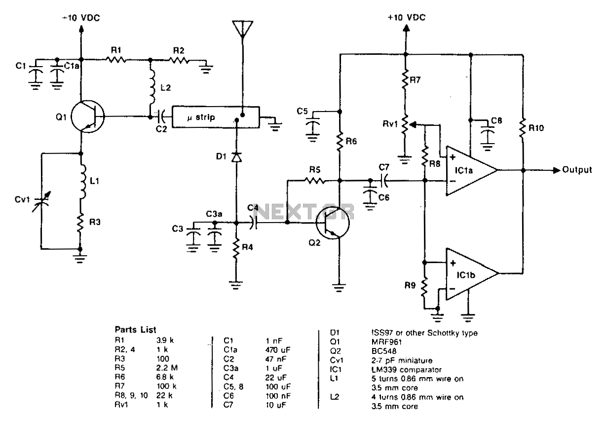
The oscillator is a standard UHF design that delivers approximately 10 mW at a frequency of 1.2 GHz. Resistors R1 and R2 bias the base of transistor Q1 to 1.2 V through a 12-ohm resistor. The collector current is set by resistor R3 to around 30 mA. Capacitor C2 couples the base of Q1 to the stripline circuit. Tuning is provided by capacitor CV1, while capacitors C1 and C1a are used for decoupling the collector. Resistors R2 and R3 are not decoupled, as this could lead to instability.
Q2 functions as a simple one-transistor amplifier. Capacitors C4 and C7 limit the gain to below 1.5 and above 100 Hz, allowing only the desired frequency band to be amplified and sent to the level detector. Two comparators, IC1, are responsible for level detection. The trigger voltage is adjustable from 8 to 60 mV using resistors R7, RV1, R8, and R9. Positive voltage swings that exceed the trigger level cause the output of IC1a to drop low, while negative swings result in a low output from IC1b. Capacitor C8 decouples IC1 from the power supply, and resistor R10 serves as a pull-up resistor for the open collector output of IC1.
The circuit described consists of a UHF oscillator and a level detection system, designed for operation at 1.2 GHz. The oscillator's output power of approximately 10 mW is achieved through careful biasing and current regulation. The use of resistors R1 and R2 ensures that the base of transistor Q1 is properly biased, allowing for stable operation. The choice of a 12-ohm resistor for the biasing network indicates a design that aims to minimize power loss while maintaining the necessary operating conditions for Q1.
The coupling between the oscillator and the stripline circuit is facilitated by capacitor C2, which plays a critical role in maintaining signal integrity while allowing the desired frequency components to pass through. Tuning is accomplished via capacitor CV1, which can be adjusted to optimize the oscillator's performance at the desired frequency.
In the amplification stage, Q2 serves to boost the signal level, with capacitors C4 and C7 strategically placed to filter out unwanted frequencies. This filtering ensures that only the frequency band of interest is amplified, enhancing the overall performance of the circuit. The level detection is managed by the dual comparator setup using IC1, which allows for precise monitoring of the signal levels. The adjustable trigger voltage enhances the circuit's versatility, accommodating a range of input signal amplitudes.
Decoupling capacitor C8 is essential for stabilizing the power supply to IC1, preventing fluctuations that could impact the performance of the level detection system. The pull-up resistor R10 ensures that the output from IC1 maintains a defined logic level, which is crucial for interfacing with subsequent stages of the circuit or external systems. Overall, this design exhibits a thoughtful approach to high-frequency signal processing and level detection, suitable for a variety of applications in communications and signal processing.The oscillator is a standard UHF design which delivers about 10 mW at 1.2 GHz. R1 and R2 bias the base of Q1 to 1.2 V via 12. Collector current is set by R3 to about 30 mA. C2 couples the base of Q1 to the stripline circuit. Tuning is provided by CVl, and C1 plus C1a decouple the collector. R2 and R3 are not decoupled, since this could cause instability. Q2 is a simple one-transistor amplifier. C4 and C7 reduce gain below 1.5 and above 100 Hz; the remaining band of frequencies is amplified and passed on to the level detector. Two comparators of IC1 provide level detection. The trigger voltage is set by R7, Rvl, R8, and R9; it is adjustable from 8 to 60 mV by Rvl. Positive voltage swings above the trigger level cause the IC1a output to become low, while negative swings cause IC1b to become low.
C8 decouples IC1 from the power supply, and RlO is a pull-up resistor for the open collector output of IC1. 🔗 External reference