
ultra low drop linear voltage regulator
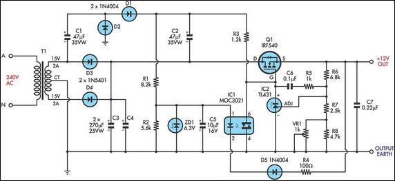
The MOSFET-based linear voltage regulator circuit is designed for efficient voltage regulation with minimal voltage drop, making it suitable for applications where low dropout and high current capability are essential. The IRF540 N-channel MOSFET is selected for its high current handling and low on-resistance characteristics, which contribute to the overall efficiency of the design. The use of a 15V-0-15V transformer allows for a sufficient input voltage range, ensuring that the MOSFET operates within its optimal range while providing a stable 12V output.
The voltage doubler circuit, consisting of diodes D1 and D2 along with capacitors C1 and C2, effectively generates the required gate drive voltage. This configuration is critical for ensuring that the MOSFET is fully enhanced, allowing it to conduct with minimal resistance. The TL431 adjustable shunt regulator serves as a feedback mechanism, continuously monitoring the output voltage and adjusting the gate drive voltage accordingly to maintain the desired output level. The inclusion of a trimpot (VR1) allows for precise tuning of the output voltage, accommodating variations in load and input voltage.
The error amplifier compensation network, formed by resistor R5 and capacitor C6, stabilizes the feedback loop, preventing oscillations and ensuring smooth operation across various load conditions. The short-circuit protection mechanism is a vital safety feature, preventing damage to the circuit during fault conditions. The use of the MOC3021 triac optocoupler provides electrical isolation between the control and power sections of the circuit, enhancing reliability and safety.
Overall, this circuit exemplifies a robust design for a linear voltage regulator, combining high efficiency, precise voltage regulation, and essential protection features, making it ideal for various electronic applications requiring stable power supply.This circuit is a Mosfet-based linear voltage regulator with a voltage drop of as low as 60mV at 1A. The circuit uses a 15V-0-15V transformer and employs an IRF540 N-channel Mosfet (Q1) to deliver the regulated 12V output. The gate drive voltage required for the Mosfet is generated using a voltage doubler circuit consisting of diodes D1 & D2 and c
apacitors C1 & C2. To turn the Mosfet fully on, the gate terminal should be around 10V above the source terminal which is connected to the DC output. The voltage doubler feeds this voltage to the gate via resistor R3. IC2, a TL431 adjustable shunt regulator, is used as the error amplifier. It dynamically adjusts the gate voltage to maintain the regulation at the output. With an adequate heatsink for the Mosfet, the circuit can provide up to 3A output at slightly elevated minimum voltage drop.
Trimpot VR1 is used for fine adjustment of the output voltage. The RC network consisting of R5 and C6 provides error-amplifier compensation. The circuit is provided with short-circuit crowbar protection to guard against an accidental short at the output. This crowbar protection works as follows: under normal working conditions, the voltage across capacitor C5 will be 6.
3V and diode D5 will be reverse-biased by the output voltage of 12V. However, during output short-circuit conditions, the output will momentarily drop, causing D5 to conduct. This triggers the MOC3021 Triac optocoupler (IC1) which in turn pulls the gate voltage to ground. This limits the output current. The circuit will remain latched in this state and the input voltage has to be switched off to reset the circuit.
🔗 External reference
Related Circuits
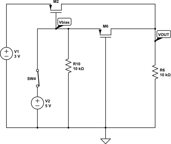
The output voltage (VOUT) is intended to be 3V when the switch is open and 5V when the switch is closed. The simulation correctly reflects the desired outcome when the switch is open; however, it does not perform as...

The amplifier feeding the final amplification stage operates with unstabilized voltage. The output stage, utilizing push-pull operation, exhibits significant rejection of the supply voltage. However, the earlier stages do not provide the same level of rejection, resulting in unwanted...
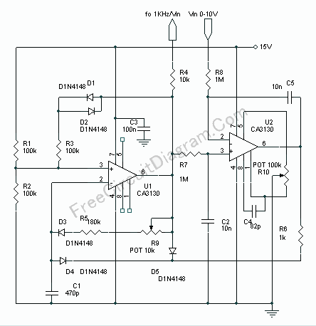
Voltage to frequency conversion is highly beneficial in various applications, such as transmitting temperature measurements using standard voice radio transceivers. This circuit utilizes two CA3130 operational amplifiers, demonstrating satisfactory performance. The linearity of the voltage-frequency transfer is better than...
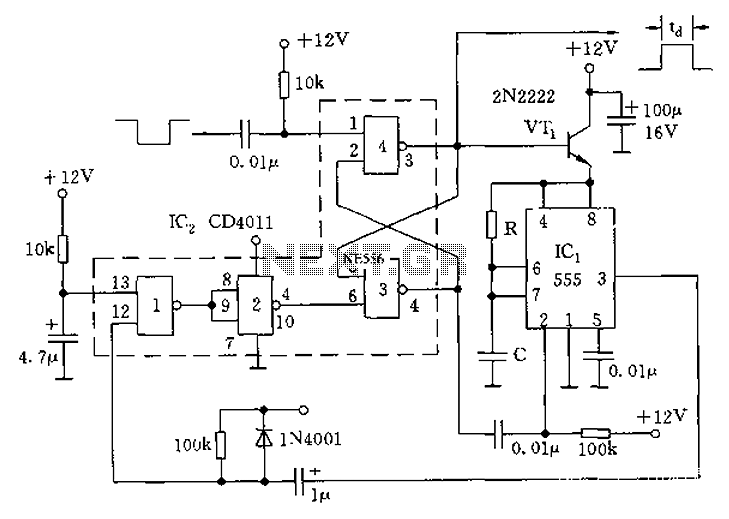
The circuit consists of four 2-input NAND gates and a CMOS CD4011 type 555 timer, allowing for either a static or high-time period output while maintaining minimal power consumption. Additionally, the circuit features a 3-door and 4-door composition RS...
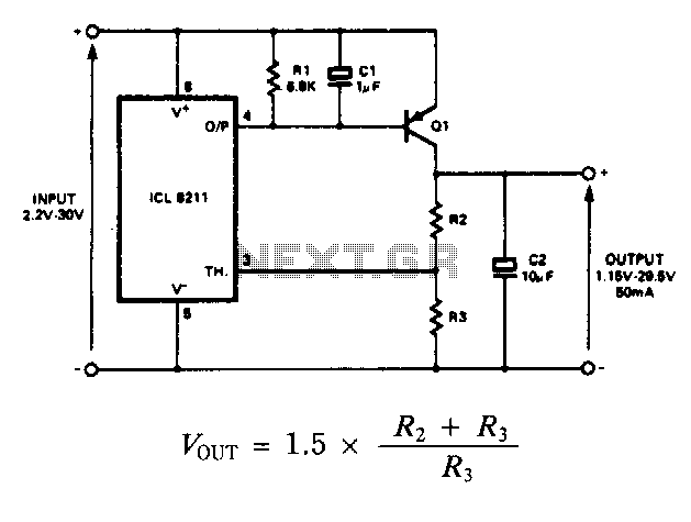
The IC8211 serves as the voltage reference and regulator amplifier, with Q1 functioning as the series pass transistor. Resistor R1 defines the output current of the IC8211, while capacitors C1 and C2 ensure loop stability and help suppress the...
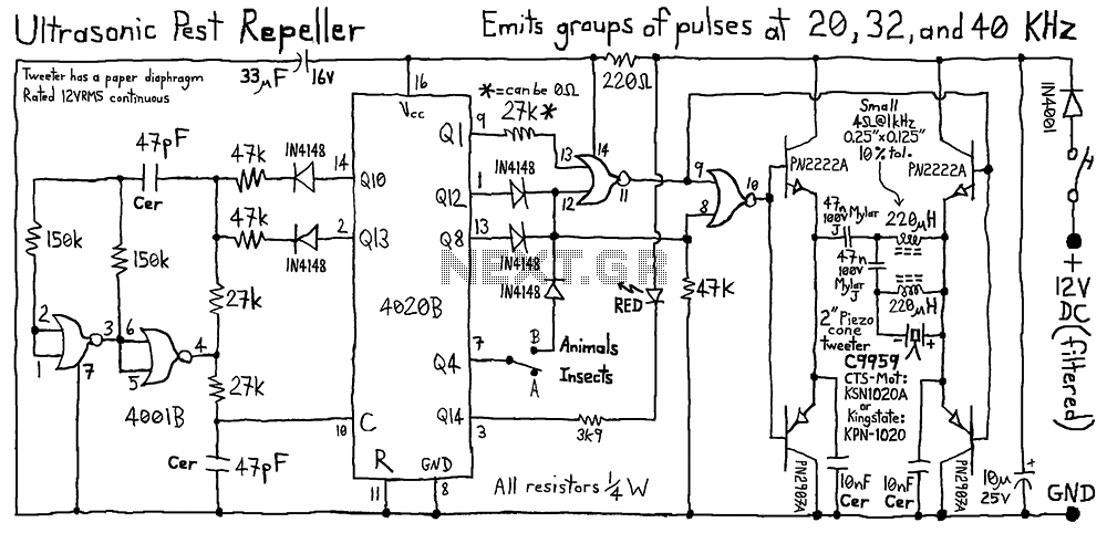
A higher-end version of the same device, featuring additional user-selectable settings to enable both audible and ultrasonic output, enhancing its effectiveness against animals. The described device is an advanced electronic system designed to produce sound waves at both audible and...
Warning: include(partials/cookie-banner.php): Failed to open stream: Permission denied in /var/www/html/nextgr/view-circuit.php on line 713
Warning: include(): Failed opening 'partials/cookie-banner.php' for inclusion (include_path='.:/usr/share/php') in /var/www/html/nextgr/view-circuit.php on line 713