
USB and GLCD Expansion Board for 8051SBC

The circuit described integrates a USB interface and a graphic LCD controller into the 8051SBC system, utilizing programmable logic devices (PLDs) for address decoding. The USB chip operates within a specified address range, allowing for efficient data transfer between the microcontroller and the USB interface. The schematic illustrates the connections between the 8051 microcontroller, the USB chip, and the GLCD controller, ensuring that the appropriate control signals are generated based on the address lines.
The PLD decoder simplifies the design by consolidating the glue logic required for enabling the various components. The use of a universal PCB layout allows for flexibility in the design and ease of manufacturing. Each connector is clearly defined, with J4 connecting to the USB board, J3 to the GLCD, and J2 providing an interface for expansion. The manual switch for the backlight enhances user control over the display.
The FT245BM USB chip provides a robust communication interface, supporting both USB 1.1 and USB 2.0 protocols, making it suitable for a wide range of applications. The graphic LCD, equipped with the KS1208 or HD61202 controller, facilitates rich visual output, with internal registers easily accessible through direct memory addressing.
The software component is integral to the functionality of the circuit, allowing for BMP file display and real-time data transmission to and from a connected PC. The interrupt-driven approach for data reception enhances responsiveness, while the ability to send ASCII data provides an interactive user experience. Overall, the circuit design effectively combines hardware and software elements to create a versatile and user-friendly system.The enable signal for USB chip and GLCD controller were made by PLD decoder from the address lines. As we have seen the memory map for i/o of 8051SBC board, the available space is from 0x0300-0x07FF. The address range of 0x0300-0x03FF was used for USB chip for both RD and WRITE operations. The GLCD used 0x0400-0x04FF with A0-A3 for selecting the i nternal registers from 0x0404-0x040B. We have learned from 8051SBC on how to use PLD as the memory decoder. In the schematic you may see the equivalent logic symbol for each enable signal. Let study the logic equation shown in Figure 3 and the equivalent logic circuit, you will understand how easy it is. Figure 4 shows the sample layout made by universal pcb. We see that with a PLD, the glue logic will be put together in PLD chip. The left-hand, J4 is 26-pin connector for USB board. And the bottom connector, J3 is 20-pin SIP connector for GLCD board. The right-hand connector J2 is for 8051SBC expansion header. Upper is manual switch for backlight turn on/off. Figure 3 shows the USB module made by Astron Logic Company. The evaluation kit consists of USB board, user manual, cable and software CD for driver and test software.
The kit is available at low-cost, to get it please contact Astron Logic directly. The USB board is based on FT245BM. The chip provides complete hardwire USB protocol that conforms USB1. 1 and USB 2. 0 (full speed mode). The FT245BM can learn more from Future Technology Devices International: FTDI. The graphic LCD is based on Samsung KS1208 or Hitachi HD61202 controller. The address of internal registers were mapped into external memory from 0x0404-0x040B. To access them we can use pointer with absolute address directly. The testing code is just display BMP file. However some function can be modified for the application purpose. More sample code and GLCD datahsheet can get from 128x64 Graphic routines and tools for GLDC. When TXE signal becomes LOW it indicates that the FIFO buffer is available for data to be received. In the main code it test P3. 3 with 0x08 MASK byte to AND with P3. If it low, the variable n will write to usb buffer through the pointer *usb_port. On receiving, instead of polling TXE signal, the RXF signal was tied to INT0 pin. When RXF actives, it will make interrupt ex0 to service. The data was read easily with pointer *usb_port. We can see the data shows on the on board text LCD. To test with host PC, the enclosed CD has test software. When we tie usb connector of the expansion board to a PC`s usb port. We can select device then. After open the device, when we press S2, it will send data to PC and the received window will show the byte being received, e. g. 0, 1, 2, 3, 4, 5, 6, . Also for sending, you can type text in Send immediate window, the ASCII letter will show on 8051SBC`s LCD while typing!
The graphic LCD test code is now under developing. I will put it when available soon. Below sample code for GLCD is just to print the three images with delay one by one. 🔗 External reference
Related Circuits

ZTEX USB-FPGA Boards require three different voltages: 1.2V, 2.5V-2.6V, and 3.3V, which must be supplied externally. This can be achieved using Power Supply Modules, Experimental Boards, or a user-specific design. To facilitate development in the latter scenario, three reference...
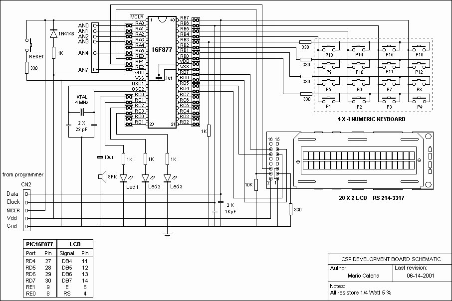
A schematic of a board featuring the PIC16F84 microcontroller, along with other compatible PIC microcontrollers that can be connected to the USB PICKit2 programmer. Additionally, there are concerns regarding the potential damage to the programmer when experimenting with oscillator...
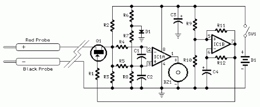
Acoustic check of transistor and diode junctions. Also suitable as a continuity tester. Short circuits or broken PCB tracks can be easily recognized. The acoustic check of transistor and diode junctions is a method used to assess the functionality of...
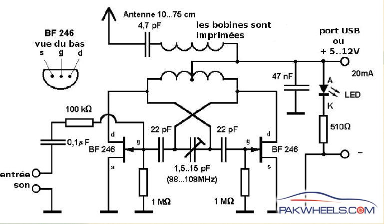
A USB-powered laptop FM transmitter designed for home theater systems and other woofers equipped with FM receivers. It transmits music from a laptop to the sound system in a room. The USB-powered laptop FM transmitter operates by converting audio signals...
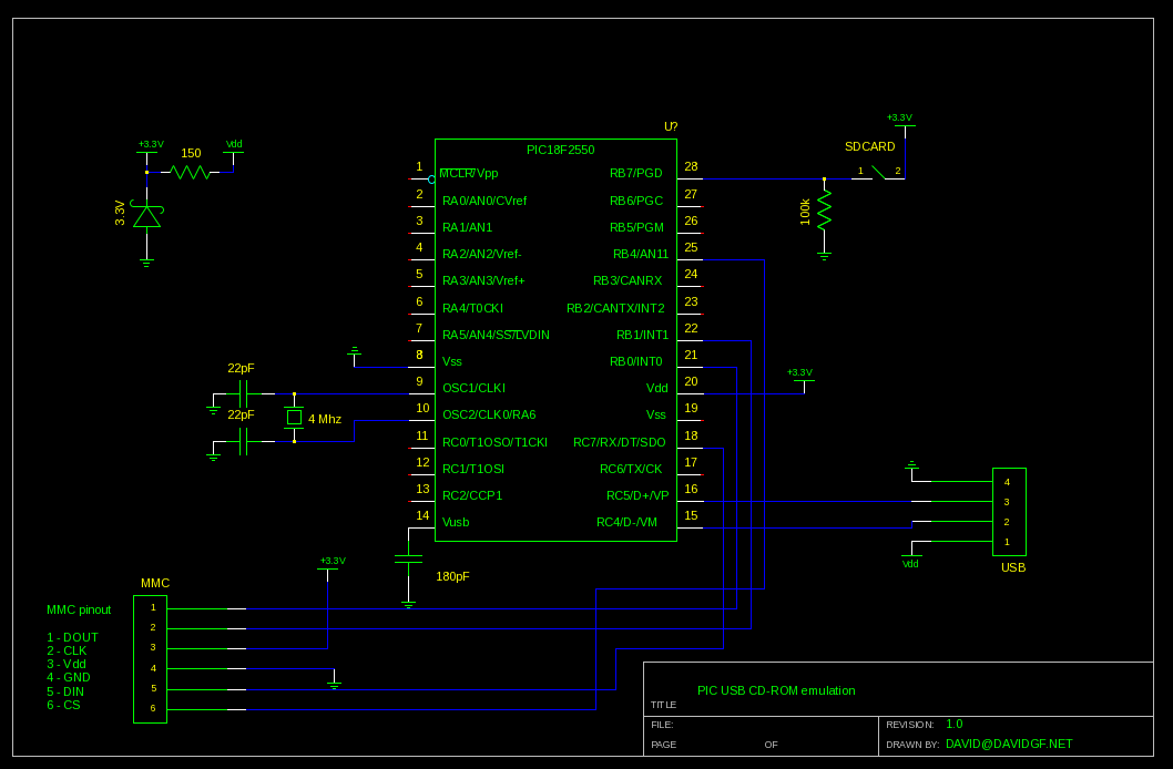
This project aims to create a USB CD-ROM device. Unlike typical devices that imitate a CD-ROM drive, this project emulates one. The concept allows users to store an ISO image or other types of CD-ROM images on an SD...

Illuminate your tabletop with this stylish White LED Lamp. It is powered through a USB port, making it perfect for taking notes while browsing the internet. The USB port can provide a convenient power source. The White LED Lamp is...