Varactor Diodes
1. Definition and Basic Principle
Varactor Diodes: Definition and Basic Principle
A varactor diode, also known as a varicap diode or voltage-variable capacitor diode, is a semiconductor device whose junction capacitance varies with the applied reverse bias voltage. Unlike conventional diodes optimized for rectification, varactors exploit the voltage-dependent width of the depletion region to function as electrically tunable capacitors.
Physical Operating Principle
The capacitance-voltage relationship arises from the modulation of the depletion region in a reverse-biased p-n junction. Under reverse bias, majority carriers are pulled away from the junction, widening the depletion region and reducing capacitance. The governing equation for the junction capacitance Cj is derived from Poisson's equation and the abrupt junction approximation:
where:
- Cj0 = zero-bias junction capacitance
- V = applied reverse bias voltage (negative for reverse bias)
- φ0 = built-in potential (typically 0.5–0.9V for silicon)
- γ = grading coefficient (0.5 for abrupt junctions, 0.33 for linear graded junctions)
Material Considerations
Modern varactors use hyperabrupt doping profiles (γ ≈ 0.5–2) to achieve steeper capacitance-voltage characteristics. Gallium arsenide (GaAs) varactors exhibit higher Q-factors than silicon at microwave frequencies due to lower series resistance. Heterojunction varactors (e.g., AlGaAs/GaAs) further enhance tuning range through bandgap engineering.
Practical Parameter Space
Key performance metrics include:
- Tuning ratio: Cmax/Cmin (typically 2:1 to 10:1 for commercial devices)
- Q-factor: >100 at 1 GHz for GaAs varactors
- Breakdown voltage: 15–60V for RF applications
The capacitance-voltage characteristic exhibits nonlinearity, necessitating Taylor series analysis for small-signal applications:
This nonlinearity generates harmonic distortion, which becomes significant in wideband voltage-controlled oscillators (VCOs) and requires compensation in precision RF systems.
1.2 Symbol and Circuit Representation
The varactor diode, also known as a voltage-variable capacitor or varicap diode, is represented in circuit schematics by a modified diode symbol that emphasizes its capacitive behavior. The standard symbol consists of a conventional diode shape with a capacitor-like addition at the cathode end, distinguishing it from rectifier or signal diodes.
Key Symbol Features
- Anode (A): Represented by the triangle (arrow) in the symbol, analogous to a standard diode.
- Cathode (K): Modified with parallel lines resembling a capacitor plate, indicating the junction capacitance.
- Biasing: Unlike conventional diodes, varactors are typically reverse-biased, with the anode at a lower potential than the cathode.
Equivalent Circuit Model
Under reverse bias, a varactor's behavior is modeled by a voltage-dependent capacitance Cj(V) in parallel with a series resistance Rs (representing bulk semiconductor resistance) and a shunt resistance Rp (modeling leakage current). The small-signal equivalent circuit includes:
where Cj0 is the zero-bias capacitance, φ is the built-in potential (~0.7V for Si), V is the applied reverse bias, and n is the grading coefficient (0.5 for abrupt junctions, 0.33 for graded).
Practical Implementation Notes
In RF circuits, varactors are often paired with inductors to form voltage-controlled oscillators (VCOs). The symbol's capacitor emphasis directly correlates with the diode's role in LC tank circuits, where the capacitance tuning range (Cmax/Cmin) determines the frequency agility. Modern SPICE models (e.g., BSIM4) incorporate these nonlinear effects through physics-based parameters like:
where Q defines the diode's quality factor at operating frequency f.
1.3 Key Electrical Characteristics
Capacitance-Voltage Relationship
The fundamental property of a varactor diode is its voltage-dependent junction capacitance, governed by the abrupt or graded doping profile. For an abrupt junction, the capacitance C as a function of reverse bias VR is derived from Poisson's equation:
where C0 is the zero-bias capacitance, φ is the built-in potential (~0.7V for Si), and n is the grading coefficient (0.5 for abrupt junctions, 0.33 for linearly graded). Hyperabrupt junctions exhibit n > 0.5, enabling wider tuning ranges in VCO applications.
Quality Factor (Q)
The quality factor quantifies energy storage efficiency at RF frequencies:
where Rs is the series resistance. High-Q (>100 at 1 GHz) is critical for low-phase-noise oscillators. Epitaxial silicon varactors achieve Q~200 at 2 GHz, while GaAs devices exceed 500 due to lower Rs.
Tuning Ratio and Linearity
The capacitance ratio Cmax/Cmin defines the tuning range. Commercial varactors typically achieve 2:1 to 10:1 ratios. For phase-locked loops, linear C-V characteristics (achieved through doping profile engineering) reduce distortion in the error signal.
Breakdown Voltage
The reverse breakdown voltage VBR limits the maximum tuning range. It's empirically related to doping concentration Nd:
where Eg is the bandgap. Si varactors typically withstand 15-30V, while GaN devices exceed 100V for high-power RF applications.
Temperature Coefficients
The temperature dependence of capacitance arises from:
- Bandgap variation (~2mV/°C for Si)
- Thermal expansion altering doping densities
- Carrier freeze-out in wide-bandgap materials
Compensation techniques include series/parallel combinations with opposite TC or monolithic integration with temperature-stable inductors.
Noise Mechanisms
Flicker noise (1/f) in varactors modulates oscillator phase noise. The noise power spectral density follows:
where Kf is the flicker noise coefficient (10-22 to 10-24 F2/Hz for Si) and α ≈ 1. Low-noise designs use guard rings and optimized passivation layers to suppress surface states.
2. Voltage-Dependent Capacitance
2.1 Voltage-Dependent Capacitance
The capacitance of a varactor diode is fundamentally governed by the width of its depletion region, which varies with the applied reverse bias voltage. Unlike conventional diodes, varactors are engineered to maximize this voltage-capacitance relationship, making them essential in tuning and frequency-control applications.
Depletion Region and Junction Capacitance
Under reverse bias, the depletion region widens as the applied voltage increases, reducing the junction capacitance. This behavior is described by the abrupt junction approximation for uniformly doped diodes:
where:
- Cj is the junction capacitance,
- Cj0 is the zero-bias capacitance,
- VR is the reverse bias voltage,
- φ0 is the built-in potential (typically 0.7–1.2 V for silicon),
- γ is the grading coefficient (0.5 for abrupt junctions, 0.33 for linearly graded junctions).
Grading Coefficient and Doping Profile
The value of γ depends on the doping profile:
- Abrupt junctions (step doping) yield γ = 0.5, ideal for high tuning sensitivity.
- Hyperabrupt junctions (engineered doping) achieve γ > 0.5, enabling near-linear frequency-voltage response in VCOs.
where m describes the doping gradient. Hyperabrupt designs use m < 0 to invert the capacitance-voltage slope.
Practical Implications
The voltage-capacitance nonlinearity introduces harmonic distortion in RF systems. Designers mitigate this by:
- Operating within limited voltage ranges,
- Using back-to-back diode configurations for symmetric tuning,
- Selecting hyperabrupt varactors for wideband VCOs requiring linear f-V characteristics.
Temperature Dependence
The built-in potential φ0 decreases with temperature (~2 mV/°C for silicon), causing capacitance drift. Compensation techniques include:
- Temperature-stabilized bias networks,
- Differential pair configurations,
- GaAs varactors for reduced thermal sensitivity in high-frequency systems.
2.2 Depletion Region and Capacitance Variation
The capacitance of a varactor diode arises from the space-charge region (depletion region) formed at the p-n junction under reverse bias. As the reverse voltage increases, the depletion region widens, reducing the junction capacitance. This voltage-dependent behavior is governed by the principles of semiconductor physics and can be derived from Poisson's equation.
Depletion Width and Applied Voltage
The width of the depletion region (W) depends on the applied reverse bias (VR) and the built-in potential (Vbi). For an abrupt junction, the depletion width is given by:
where εs is the semiconductor permittivity, q is the electron charge, and NA and ND are the acceptor and donor concentrations, respectively.
Junction Capacitance Derivation
The junction capacitance (Cj) is modeled as a parallel-plate capacitor with the depletion region acting as the dielectric. The capacitance per unit area is inversely proportional to the depletion width:
Substituting the expression for W yields the voltage-dependent capacitance:
where Cj0 is the zero-bias junction capacitance. For hyperabrupt junctions, the doping profile is engineered to achieve a steeper capacitance-voltage relationship:
where n ranges from 0.5 (abrupt junction) to >1 (hyperabrupt).
Practical Implications
In RF applications, varactors are operated in reverse bias to minimize conductive losses. The tuning ratio (Cmax/Cmin) is a critical figure of merit, determined by the doping profile and breakdown voltage. Modern varactors achieve tuning ratios exceeding 10:1 using epitaxial growth techniques to precisely control the doping gradient.
Non-Ideal Effects
- Series resistance: Arises from undepleted semiconductor regions, limiting the quality factor (Q) at high frequencies
- Temperature dependence: Vbi decreases with temperature (~2 mV/°C for silicon)
- Nonlinear distortion: Higher-order terms in the C-V relationship generate harmonics in tuning applications
2.3 Reverse Bias Operation
Varactor diodes operate exclusively under reverse bias, where the applied voltage increases the depletion region width, modulating the junction capacitance. Unlike forward bias, which induces high conduction current, reverse bias ensures minimal leakage current while enabling precise voltage-controlled capacitance tuning.
Depletion Region and Capacitance Modulation
Under reverse bias (VR > 0), the depletion region widens as majority carriers are pushed away from the junction. The resulting capacitance (Cj) follows the abrupt junction approximation for a one-sided step junction:
where:
- Cj0 is the zero-bias junction capacitance,
- φ0 is the built-in potential (typically 0.7–1.2 V for silicon),
- n is the grading coefficient (0.5 for abrupt junctions, 0.33 for linear graded junctions).
The nonlinear relationship between Cj and VR is critical for frequency tuning applications, such as voltage-controlled oscillators (VCOs).
Breakdown Voltage and Practical Limits
As reverse bias increases, the electric field across the depletion region intensifies. At the breakdown voltage (VBR), impact ionization triggers avalanche breakdown, causing uncontrolled current flow. Varactors are designed to operate well below VBR, with typical working ranges of 5–30 V for silicon and 15–60 V for GaAs devices.
Quality Factor (Q) and Series Resistance
The quality factor quantifies energy loss and is frequency-dependent:
where Rs is the series resistance (dominated by undepleted epitaxial layer resistance). High-Q varactors (Q > 100 at 1 GHz) are essential for low-phase-noise oscillators. Advanced fabrication techniques, such as hyperabrupt doping profiles, optimize Q by minimizing Rs.
Temperature Dependence
The reverse-bias capacitance exhibits temperature sensitivity due to:
- Carrier concentration shifts: Dopant ionization varies with temperature, altering φ0.
- Thermal expansion: Lattice constant changes modify the relative permittivity.
Compensation techniques include using temperature-stable dopants (e.g., platinum in silicon) or differential pair configurations in circuit designs.
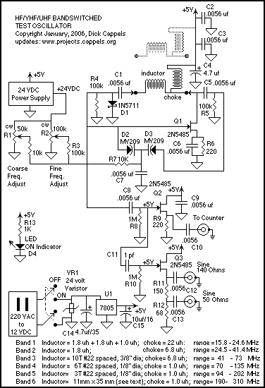
Applications in Tuning Circuits
Reverse-biased varactors enable:
- VCOs: Frequency modulation via voltage-controlled capacitance in LC tanks.
- Phase-locked loops (PLLs): Dynamic frequency adjustment for synchronization.
- RF filters: Adaptive bandwidth tuning in communication systems.
3. Tuning Circuits in RF Applications
3.1 Tuning Circuits in RF Applications
Varactor diodes serve as voltage-controlled capacitors in radio frequency (RF) tuning circuits, enabling precise frequency adjustments without mechanical components. Their nonlinear capacitance-voltage (C-V) characteristic allows them to replace traditional variable capacitors in oscillators, filters, and phase-locked loops (PLLs). The capacitance C(v) of a varactor diode is governed by:
where C0 is the zero-bias capacitance, v is the reverse bias voltage, φ is the built-in potential (~0.7 V for silicon), and n is the junction grading coefficient (0.5 for abrupt junctions, 0.33 for graded).
Resonant Frequency Tuning
In an LC tank circuit, the resonant frequency fr is modulated by varying the varactor’s capacitance:
For a series resonant circuit, the quality factor Q is critical for selectivity and is expressed as:
where R represents the equivalent series resistance (ESR) of the diode and inductor. High-Q varactors (e.g., gallium arsenide (GaAs) types) minimize losses in RF front-ends.
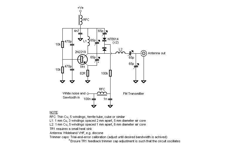
Practical Implementation in VCOs
Voltage-controlled oscillators (VCOs) leverage varactors for frequency agility. A Colpitts oscillator with a varactor tuning network exemplifies this:
The tuning range Δf is constrained by the varactor’s capacitance ratio Cmax/Cmin and the circuit’s parasitic capacitances. For a 1:3 capacitance ratio, the theoretical frequency ratio is:
Linearity and Distortion Mitigation
Varactor nonlinearity introduces harmonic distortion in wideband tuning. Predistortion techniques or back-to-back diode configurations improve linearity by canceling even-order harmonics. The effective capacitance of a back-to-back pair becomes:
Temperature stability is another critical factor; silicon varactors exhibit a temperature coefficient of ~100 ppm/°C, while GaAs variants offer better performance (~30 ppm/°C).
Case Study: FM Transmitter Tuning
In FM transmitters, varactors modulate the carrier frequency directly. A 100 MHz VCO with a varactor tuning sensitivity of 10 MHz/V requires a capacitance swing of 2.5 pF to 10 pF for ±75 kHz deviation, adhering to FCC bandwidth regulations.
3.2 Voltage-Controlled Oscillators (VCOs)
Fundamental Operating Principle
The core function of a voltage-controlled oscillator (VCO) is to generate an output signal whose frequency is a function of an applied control voltage. Varactor diodes serve as the key tuning element, leveraging their voltage-dependent capacitance to adjust the resonant frequency of an LC tank circuit. The relationship between the control voltage Vctrl and the output frequency fout is given by:
where L is the fixed inductance and C(Vctrl) is the varactor's junction capacitance, which varies nonlinearly with Vctrl.
Varactor Tuning Characteristics
The capacitance-voltage (C-V) relationship of a varactor diode is derived from the abrupt or hyperabrupt junction doping profiles. For an abrupt junction, the capacitance follows:
where Cj0 is the zero-bias capacitance, Vbi is the built-in potential (~0.7 V for silicon), and γ is the grading coefficient (0.5 for abrupt junctions, 0.5–2 for hyperabrupt). Hyperabrupt varactors provide a more linear fout vs. Vctrl response, critical for wide-tuning-range VCOs.
Circuit Topologies
Colpitts VCO with Varactor Tuning
A common implementation uses a Colpitts oscillator with the varactor placed in parallel with the tank circuit. The feedback network (capacitors C1 and C2) sets the oscillation condition, while the varactor adjusts the resonant frequency. The effective tank capacitance becomes:
Negative Resistance VCOs
At microwave frequencies, negative-resistance oscillators (e.g., using Gunn diodes) paired with varactors enable tuning ranges exceeding 10 GHz. The Kurokawa stability criterion must be satisfied to ensure sustained oscillations.
Phase Noise Considerations
Phase noise in VCOs is dominated by the Leeson effect, modeled as:
where QL is the loaded quality factor of the tank, and Δf1/f³ is the flicker noise corner frequency. Varactors contribute to phase noise through their Q-factor and flicker noise, necessitating high-Q hyperabrupt designs for low-noise applications.
Practical Design Example
A 2.4 GHz VCO for Wi-Fi 6E might use a SMV1234 hyperabrupt varactor (Cj0 = 2.2 pF, γ = 0.9) with a 5 nH inductor. For Vctrl = 0–5 V, the tuning range is:
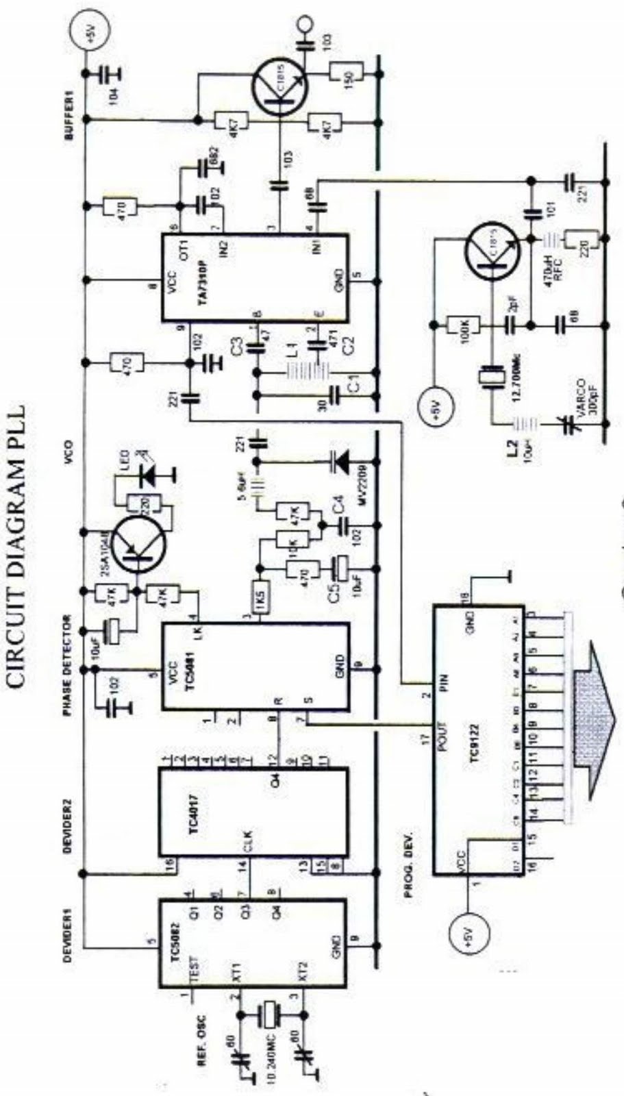
Applications
- Phase-locked loops (PLLs): Varactor-based VCOs are integral to frequency synthesis in RF transceivers.
- Radar systems: Fast tuning enables frequency-modulated continuous-wave (FMCW) operation.
- Test equipment: Sweep generators leverage wide-tuning-range VCOs for stimulus signals.
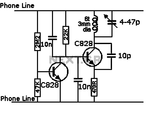
3.3 Frequency Modulators and Phase Shifters
Varactor Diodes in Frequency Modulation
Varactor diodes, also known as varicap diodes, exploit voltage-dependent capacitance to enable frequency modulation (FM) in RF circuits. The junction capacitance \( C_j \) of a varactor diode varies with the applied reverse bias voltage \( V_R \), following the relationship:
where \( C_0 \) is the zero-bias capacitance, \( \phi \) is the built-in potential (~0.7V for silicon), and \( n \) is the doping profile exponent (typically 0.5 for abrupt junctions, 0.33 for graded junctions). In FM applications, the modulating signal \( V_m(t) \) is superimposed on the DC bias \( V_{DC} \), causing a time-varying capacitance:
When integrated into an LC tank circuit, this modulates the resonant frequency \( f_r \):
Phase Shifting with Varactors
Varactors enable precise phase control in RF systems by altering the propagation delay through a transmission line or resonator. In a reflection-type phase shifter, a varactor-terminated transmission line reflects signals with a phase shift \( \Delta \phi \) given by:
where \( Z_0 \) is the characteristic impedance of the line. For small phase shifts (\( \Delta \phi \ll \pi/2 \)), this simplifies to:
Practical implementations often use quadrature hybrid couplers with varactor-loaded branches to achieve 0°–180° continuous phase tuning while maintaining impedance matching.
Nonlinearity and Distortion
The nonlinear \( C_j(V_R) \) characteristic introduces harmonic distortion in wideband FM systems. The third-order intermodulation distortion (IMD3) can be derived from a Taylor expansion of \( C_j \):
This necessitates careful bias point selection and predistortion techniques in high-linearity applications like cellular base stations.
Practical Implementation Example
A common VCO (Voltage-Controlled Oscillator) topology using a Clapp oscillator with varactor tuning:
The tuning sensitivity \( K_V \) (Hz/V) is determined by:
Modern implementations often use hyperabrupt junction varactors (n ≈ 0.75–1.5) for improved linearity and tuning range.
4. Capacitance Ratio (Cmax/Cmin)
4.1 Capacitance Ratio (Cmax/Cmin)
The capacitance ratio (Cmax/Cmin) is a critical figure of merit for varactor diodes, defining their tuning range in voltage-controlled applications. This ratio quantifies the maximum achievable variation in junction capacitance as a function of applied reverse bias voltage. A higher ratio allows for broader frequency tuning in oscillators, filters, and phase-locked loops.
Mathematical Derivation of Capacitance Ratio
The junction capacitance Cj of a varactor diode follows the relationship:
where:
- Cj0 is the zero-bias junction capacitance,
- V is the applied reverse bias voltage,
- V0 is the built-in potential (typically 0.5–0.9 V for silicon),
- n is the grading coefficient (0.5 for abrupt junctions, ~0.33 for hyperabrupt).
The maximum capacitance Cmax occurs at zero bias (V = 0), reducing to:
The minimum capacitance Cmin is achieved at the maximum rated reverse bias Vmax:
Thus, the capacitance ratio simplifies to:
Practical Implications
For abrupt junction varactors (n = 0.5), a Vmax of 20 V and V0 of 0.7 V yields:
Hyperabrupt designs (n ≈ 0.33) trade reduced ratio for linearized tuning characteristics. Modern GaAs varactors achieve ratios exceeding 10:1, enabling wideband RF applications.
Trade-offs and Design Considerations
- Breakdown voltage: Higher Vmax improves the ratio but requires robust doping profiles.
- Q factor: Thin epitaxial layers increase Cmax/Cmin but may degrade resonator quality.
- Temperature stability: The ratio exhibits positive temperature coefficients (~100 ppm/°C) due to V0 dependence.
4.2 Quality Factor (Q)
The quality factor (Q) of a varactor diode quantifies its efficiency in storing and releasing energy at a given frequency. It is a critical parameter in tuning circuits, oscillators, and filters, where high Q values indicate lower energy losses. The Q factor is defined as the ratio of the reactance to the series resistance at the operating frequency:
Here, Xs is the reactance of the varactor, Rs is the series resistance, f is the operating frequency, and Cj is the junction capacitance. A higher Q implies lower resistive losses and better frequency selectivity.
Derivation of Q for a Varactor Diode
The quality factor can be derived by analyzing the equivalent circuit of a varactor diode, which consists of a voltage-dependent capacitance Cj(V) in series with a resistance Rs (representing bulk and contact resistances). The impedance Z of the diode is:
The magnitude of the reactance |Xs| is 1/(ωCj), leading to the standard definition of Q. For practical varactors, Rs is minimized to maximize Q, especially in high-frequency applications.
Frequency Dependence of Q
The Q factor is frequency-dependent due to the interplay between Cj and Rs. At low frequencies, Q tends to be high because the reactance dominates. However, as frequency increases, parasitic effects (e.g., series inductance, skin effect) degrade Q. The cutoff frequency fc, where Q drops to unity, is a key metric:
Beyond fc, the varactor becomes ineffective as a tuning element.
Practical Implications
In voltage-controlled oscillators (VCOs) and phase-locked loops (PLLs), a high Q ensures lower phase noise and better stability. For example, in a VCO operating at 2 GHz, a varactor with Q > 50 is typically required to minimize signal degradation. Modern hyperabrupt junction varactors achieve Q values exceeding 100 at microwave frequencies by optimizing doping profiles and minimizing Rs.
Trade-offs and Limitations
While high Q is desirable, it often conflicts with other parameters like tuning range (Cmax/Cmin). Hyperabrupt varactors, for instance, offer wide tuning but at the cost of reduced Q. Designers must balance these factors based on application requirements.
The figure illustrates the typical Q-frequency relationship, showing peak Q at mid-range frequencies before parasitic effects dominate.
4.3 Breakdown Voltage and Leakage Current
Breakdown Voltage in Varactor Diodes
The breakdown voltage (VBR) of a varactor diode is the reverse-bias voltage at which the depletion region experiences avalanche or Zener breakdown, leading to a sharp increase in current. Unlike conventional diodes, varactors are optimized for capacitive tuning rather than rectification, so VBR must be carefully considered to avoid catastrophic failure in voltage-controlled oscillators (VCOs) or tunable filters.
The breakdown mechanism is governed by the electric field (E) in the depletion region. For abrupt junction varactors, the critical field strength (Ecrit) is approximated by:
where q is the electron charge, ND is the doping concentration, and ϵs is the semiconductor permittivity. Hyperabrupt junctions exhibit a lower VBR due to their nonlinear doping profile, trading off tuning range for voltage sensitivity.
Leakage Current and Reverse-Bias Behavior
Under reverse bias, varactors exhibit leakage current (IR) due to minority carrier diffusion and generation-recombination in the depletion region. This current follows the Shockley diode equation modified for reverse bias:
where IS is the saturation current, ni is the intrinsic carrier concentration, W is the depletion width, A is the junction area, and Ï„g is the generation lifetime. At high temperatures, leakage increases exponentially, degrading the diode's Q-factor in RF applications.
Practical Implications
- Voltage Margin: Operating near VBR risks thermal runaway. A safety margin of 20–30% below VBR is typical.
- Material Selection: GaAs varactors outperform silicon at high frequencies due to lower IR and higher Ecrit.
- Circuit Design: Leakage-induced phase noise in VCOs can be mitigated by biasing the varactor at the lowest usable voltage.
Measurement Techniques
Breakdown voltage is measured using a curve tracer with current compliance to prevent damage. Leakage current requires sensitive picoammeters due to its low magnitude (nA–pA range). For high-precision applications, guarding techniques eliminate parasitic currents in test fixtures.
5. Temperature Effects on Performance
5.1 Temperature Effects on Performance
The performance of varactor diodes is highly sensitive to temperature variations due to their dependence on semiconductor material properties, junction capacitance, and reverse bias characteristics. Temperature-induced changes affect key parameters such as capacitance-voltage (C-V) characteristics, quality factor (Q), and tuning linearity.
Thermal Dependence of Junction Capacitance
The junction capacitance Cj of a varactor diode is given by:
where Cj0(T) is the zero-bias capacitance, V is the applied reverse bias, φ(T) is the temperature-dependent built-in potential, and γ is the grading coefficient. The built-in potential φ(T) decreases with temperature due to increased intrinsic carrier concentration ni(T):
where α is the temperature coefficient (typically ~2 mV/°C for silicon). This results in a net increase in Cj at higher temperatures for a fixed bias voltage.
Temperature Effects on Quality Factor (Q)
The quality factor Q degrades with temperature due to increased series resistance Rs(T) and altered dielectric losses. The relationship is given by:
For silicon varactors, Rs(T) increases approximately linearly with temperature due to reduced carrier mobility:
where β ≈ 0.008 °C-1 for lightly doped silicon. At high frequencies (>1 GHz), this can lead to significant Q degradation in uncooled applications.
Tuning Nonlinearity and Temperature Compensation
Temperature-induced nonlinearity in tuning response can be mitigated through:
- Differential pair configurations using matched varactors to cancel first-order temperature drift.
- Bias current compensation in oscillator circuits, adjusting control voltage based on temperature feedback.
- Material selection (GaAs varactors exhibit lower ∂C/∂T than silicon above 100°C).
Advanced designs often integrate temperature-stable varactors with negative temperature coefficient (NTC) components to maintain consistent tuning characteristics across operating conditions.
Practical Considerations in RF Systems
In voltage-controlled oscillators (VCOs), temperature-dependent varactor behavior causes frequency drift. The normalized frequency sensitivity is:
For a typical hyperabrupt junction (γ = 0.5) at V = 5V, this results in ~100 ppm/°C frequency drift—critical in precision RF systems requiring <50 ppm stability.
5.2 Nonlinearity and Distortion
The voltage-dependent capacitance of a varactor diode inherently introduces nonlinear behavior, leading to harmonic distortion and intermodulation products in RF systems. This nonlinearity arises from the depletion region's dependence on the applied reverse bias, governed by the doping profile and semiconductor physics.
Mathematical Modeling of Nonlinear Capacitance
The junction capacitance Cj follows a power-law relationship with reverse voltage VR:
where Cj0 is the zero-bias capacitance, φ is the built-in potential (~0.7V for Si), and γ is the grading coefficient (0.5 for abrupt junctions, 0.33 for graded junctions). Expanding this as a Taylor series around the bias point V0 reveals the nonlinear terms:
where v = VR - V0 is the AC signal component, and the coefficients Cn are voltage-dependent derivatives of the capacitance function.
Harmonic Generation Mechanism
When a sinusoidal signal v(t) = Vmsin(ωt) is applied, the nonlinear capacitance produces current components at multiples of the fundamental frequency:
The quadratic (C2) and cubic (C3) terms generate second and third harmonics at 2ω and 3ω respectively. For a two-tone input at frequencies ω1 and ω2, intermodulation products appear at 2ω1 ± ω2 and 2ω2 ± ω1.
Distortion Metrics in Practical Applications
Key figures of merit for varactor linearity include:
- Third-order intercept point (IP3): Theoretical input power where third-order products equal the fundamental tone
- 1dB compression point: Input power causing 1dB gain reduction due to nonlinearity
- Spurious-free dynamic range (SFDR): Ratio between fundamental and largest distortion product
In voltage-controlled oscillators (VCOs), these nonlinearities contribute to phase noise through AM-to-PM conversion, where amplitude fluctuations modulate the varactor capacitance, creating frequency deviations.
Linearity Improvement Techniques
Several methods mitigate varactor distortion:
- Back-to-back diode configuration: Cancels even-order harmonics by exploiting symmetric nonlinearity
- Hyperabrupt doping profiles: Achieve more linear C-V characteristics through tailored impurity distributions
- Predistortion networks: Compensate nonlinearity with inverse transfer functions
- Optimal bias selection: Operating at higher reverse voltages reduces relative capacitance variation
5.3 Handling and Biasing Best Practices
Reverse Biasing and Voltage Control
Varactor diodes operate exclusively under reverse bias, where the depletion region width modulates with applied voltage, altering capacitance. The junction capacitance \( C_j \) follows:
Here, \( C_0 \) is the zero-bias capacitance, \( V_R \) is the reverse voltage, \( \phi \) is the built-in potential (~0.7 V for silicon), and \( n \) is the grading coefficient (0.5 for abrupt junctions, 0.33 for hyperabrupt). Exceeding the breakdown voltage \( V_{BR} \) causes irreversible damage.
Thermal Management
Leakage current \( I_R \) increases exponentially with temperature, degrading the quality factor \( Q \):
where \( R_s \) is the series resistance. For high-frequency applications (e.g., VCOs), maintain junction temperatures below 85°C using:
- Thermal pads with low thermal resistance (< 1°C/W).
- Active cooling in high-power designs (e.g., Peltier elements).
ESD Protection
Varactors are sensitive to electrostatic discharge (ESD) due to thin depletion layers. Mitigation strategies include:
- Using anti-static wrist straps during handling.
- Implementing Schottky diode clamps in parallel for transient suppression.
- Limiting bias voltage slew rates to < 1 V/µs to prevent dynamic breakdown.
Bias Network Design
To minimize parasitic effects in RF circuits:
- Employ high-impedance bias tees (e.g., RFC inductors > 1 µH) to isolate DC from RF signals.
- Use low-ESR decoupling capacitors (e.g., 100 nF ceramic) near the diode terminals.
where \( Z_{bias} \) should present > 1 kΩ impedance at the operating frequency.
Practical Tuning Considerations
For linear frequency tuning in VCOs, hyperabrupt varactors (\( n \approx 0.33 \)) are preferred. The tuning sensitivity \( K_V \) is:
where \( f_0 \) is the center frequency. For minimal phase noise, avoid operating near \( V_R = 0 \) due to higher \( R_s \).
6. Key Research Papers and Books
6.1 Key Research Papers and Books
- Different Types of Diodes, Ideal and Real Diodes, Switching Diodes ... — Super barrier diodes are rectiï¬er diodes that incorporate the low forward voltage drop of the Schottky diode with the surge-handling capability and low reverse leakage current of a normal p-n junction diode. 6.1.11 Varicap (or Varactor) Diodes These are used as voltage-controlled capacitors. These are important in PLL
- PDF Design Technique for Varactor Analog Phase Shifters with Equalized Losses — Progress In Electromagnetics Research C, Vol. 86, 1-16, 2018 Design Technique for Varactor Analog Phase Shifters with Equalized Losses Artem R. Vilenskiy1, 2, *, Mikhail N. Makurin1, Ekaterina I. Poshisholina1, and Chongmin Lee3 Abstract—The paper presents a novel design technique for reflection-type varactor analog phase
- PDF Design and Investigation of Microelectromechanical (MEMS) Varactors — 1.2 Varactor Applications 2 1.3 Varactor Main Characteristics 4 1.4 Semiconductor Varactors and MEMS Perspective 5 1.5 Aim of the Work 6 2. State of the Art 7 2.1 Continuous Capacity Change and Actuation Mechanisms 7 2.2 Variation of the Effective Dielectric Constant 7 2.3 Plate area Variation 8 2.4 Gap Variation 9 3.
- Different Types of Diodes, Ideal and Real Diodes, Switching Diodes ... — Part of the book series: Engineering Materials ((ENG.MAT.)) ... 6.1.11 Varicap (or Varactor) Diodes. These are used as voltage-controlled capacitors. These are important in PLL (phase-locked loop) and FLL (frequency-locked loop) circuits, allowing tuning circuits such as those in television receivers, to lock quickly, replacing older designs ...
- PDF Varactor Diode Distributed Phase Shifter - Paris Diderot University — Varactor Diode Distributed Phase Shifter Peter Timbie 26 May 2009 Most of this comes from a PhD thesis by Hongjoon Kim, entitled "Theory and Application of Righht-handed and Left-handed Nonlinear Transmission Lines," UW-Madison 2006. 1 Overview Varactor diodes change their capacitance in inverse proportion to bias voltage (see below). An
- Electronic Circuit Design and Application - Academia.edu — Text Features This book enables the reader to analyze a variety of circuits, to develop a deep understanding of their operation, and to design and optimize a range of working circuits and systems. Many examples help the reader to quickly become familiar with key design parameters and design methodology for each class of circuits.
- (PDF) A Research Assignment on Diode - Academia.edu — Figure 14. Tunnel Diode Symbol 6.9. Varactor Diode These are also known as Varicap diodes. It acts like the variable capacitor. Operations are performed mainly at reverse bias state only. These diodes are very famous due to its capability of changing the capacitance ranges within the circuit in the presence of constant voltage flow.
- PDF ABSTRACT - NASA Technical Reports Server (NTRS) — Whisker contacted GaAs Schottky varactor diodes are presently in use to supply local oscillator power at frequencies as high as 700 GHz for ground based and airborne applications [1,2,3]. These diodes are also used in the Microwave Limb Sounder on NASA's Upper Atmosphere Research Satellite which is now monitoring global ozone depletion [4].
- Microwave Diodes (Varactor Diode, p-i-n Diode, IMPATT Diode ... - Springer — 8.1.1 V-I Characteristics of Varactor Diode. As already said, varactor diode is a semiconductor device in which the junction capacitance can be varied as a function of reverse voltage (bias) of the diode (Fig. 8.2). Losses in this non-linear element are almost negligible.
- (PDF) Design Technique for Varactor Analog Phase Shifters with ... — The paper presents a novel design technique for reflection-type varactor analog phase shifters based on tunable reflective loads. The reflective load comprises two similar tuning stubs with ...
6.2 Manufacturer Datasheets
- DKV6522-12 Datasheet (PDF) - Advanced Semiconductor — Electronic Components Datasheet Search English Chinese: German : Japanese ... The ASI DKV6522-12 is an Silicon Hyperabrupt Varactor Diode Designed for VHF/UHF Filters and Oscillators Requiring Octave Tuning. ... Similar Part No. - DKV6522-12: Manufacturer: Part # Datasheet: Description: Advanced Semiconductor: DKV6522-24: 27Kb / 1P: SILICON ...
- Varactor Diodes - Mouser - Mouser Electronics — Varactor Diodes Varactor Diodes are available at Mouser Electronics. Mouser offers inventory, pricing, & datasheets for Varactor Diodes Varactor Diodes. Skip to Main Content (800) 346-6873. Contact Mouser (USA) (800) 346-6873 | Feedback. ... Manufacturer Capacitance Vr - Reverse Voltage If - Forward Current Mounting Style
- PDF VARACTOR DIODES - Mouser Electronics — VARACTOR DIODES Sprague-Goodman Electronics, Inc. 1700 SHAMES DRIVE, WESTBURY, NY 11590 ... 516-334-8700 • FAX: 516-334-8771 • E-MAIL: [email protected] VARACTOR DIODES SG-950 SUPER HYPERABRUPT TUNING VARACTOR DIODES • Low voltage wireless phase locked loop VCOs • Phase shifters ... 5.85 7.15 1.6 2.0 2.8 3.4 1200 GVD20434-001 ...
- 6.2 V Zener Diodes Datasheets - Mouser - Mouser Electronics — 6.2 V Zener Diodes are available at Mouser Electronics. Mouser offers inventory, pricing, & datasheets for 6.2 V Zener Diodes. Skip to Main Content (800) 346-6873. Contact Mouser (USA) (800) ... Manufacturers; Services & Tools; Technical Resources; Help; Menu. Account & Orders . Log In.
- Varactor Diodes Datasheets - Mouser - Mouser Electronics — Varactor Diodes are available at Mouser Electronics. Mouser offers inventory, pricing, & datasheets for Varactor Diodes. Skip to Main Content (800) 346-6873. Contact Mouser (USA) (800) 346-6873 | Feedback. ... Manufacturers; Services & Tools; Technical Resources; Help; Contact Us; Main Menu.
- DKV6522B Datasheet (PDF) - Advanced Semiconductor — Electronic Components Datasheet Search English Chinese : German ... The ASI DKV6522B is a Silicon Hyperabrupt Varactor Diode Designed for VHF/UHF Filters and Oscillators Requiring Octave Tuning. ... • CT4 = 50 pF Nominal • CT4/CT20 = 6.2 Typical • Hermetic Glass Package. Similar Part No. - DKV6522B: Manufacturer: Part # Datasheet ...
- Infineon Varactor Diodes - Mouser - Mouser Electronics — Infineon Varactor Diodes are available at Mouser Electronics. Mouser offers inventory, pricing, & datasheets for Infineon Varactor Diodes. Skip to Main Content (800) 346-6873. Contact Mouser (USA) (800) 346-6873 | Feedback. Change Location. English. Español $ USD United States. Please confirm your currency selection: Mouser Electronics ...
- VARACTOR DIODE Datasheet(PDF) - 1SV222 - Renesas Technology Corp — Searched Keyword: VARACTOR DIODE . Part #: 1SV222. Datasheet: 185Kb/4P. Description: VARACTOR DIODE. Manufacturer: Renesas Technology Corp. 44,089 Results. Part ...
- PDF SANYO Semiconductors DATA SHEET - docs.rs-online.com — SVC704 Silicon Diffused Junction Type Varactor Diode Varactor Diode for AFC, VCO SANYO Semiconductors DATA SHEET Any and all SANYO Semiconductor products described or contained herein do not have specifications ... 2.1 1.6 2.0 0.65 0.3 0.85 0.15 12 3 0 to 0.02 Interterminal Capacitance, C -- pF
- DigiKey Varactor Diodes Data Sheets | GlobalSpec - Datasheet Directory — Find DigiKey Varactor Diodes Data Sheets on GlobalSpec. 701 Brooks Avenue South Thief River Falls, MN 56701 United States
6.3 Online Resources and Tutorials
- PDF Electrical and Electronic Principles and Technology — Electrical part of 'Applied Electrical and Mechan-ical Science for Technicians' (BTEC First Certificate). Various parts of City & Guilds Technician Certificate/Diploma in Electrical and Electronic Principles/Telecommunication Systems, such as Electrical Engineering Principles, Power, and Science and Electronics.
- 2: PN Junctions and Diodes - Engineering LibreTexts — Discuss the different kinds of diodes available and their uses: rectifier, Zener, LED, photodiode and varactor. Detail the device characteristics exhibited by different diode types. Graph the forward- and reverse-bias operation regions of diodes. Determine the effective resistance of a diode under specific conditions.
- PDF Zetex Variable Capacitance Diodes — Introduction The advent of varactor diodes has made a huge impact in many areas of electronic design, which is only too evident in todays consumer products. Formerly, where bulky or unreliable mechanical methods were used, the size, reliability and excellent tracking abilities of the varactor has led to smaller, cheaper and more elaborate circuitry, previously impossible to attain.
- Lab 3 - Diodes | Instrumentation LAB — Does this diode have exactly the same forward voltage drop as the diode you used in part 3.1? Forward voltage drops vary between types of diodes and even between diodes of the same type.
- Diodes - A Practical Guide | DroneBot Workshop — Diodes are the oldest semiconductor device, and they remain one of the most important. Let's look at how diodes work and how you can use them.
- Semiconductor Devices: Theory and Application - Open Textbook Library — The goal of this text, as its name implies, is to allow the reader to become proficient in the analysis and design of circuits utilizing discrete semiconductor devices. It progresses from basic diodes through bipolar and field effect transistors. The text is intended for use in a first or second year course on semiconductors at the Associate or Baccalaureate level. In order to make effective ...
- PDF Semiconductor Diode - talkingelectronics.com — Therefore, like a vacuum diode, a semiconductor diode can also accomplish the job of rectification i.e. change alternating current to direct current. However, semiconductor diodes have become more *popular as they are smaller in size, cheaper and robust and usually operate with greater efficiency.
- 2.6: Exercises - Engineering LibreTexts — 3.6.2: Design Problems 12. Design a 15 volt AC to DC power supply capable of drawing 200 mA. 13. Design a circuit that will limit its output voltage to a range of −5 volts to +10 volts. 14. Design a circuit that will shift its output voltage so that it is always positive. The input frequency is 2 kHz.
- Chapter 6: Diode applications (Power supplies, voltage ... - Analog — Zener diodes are widely used as voltage references and as shunt regulators to regulate the voltage across small circuits. When connected in parallel with a varying voltage source, such as the diode rectifier we just discussed, so that it is reverse biased, the zener diode conducts when the voltage reaches the diode's reverse breakdown voltage.
- Lessons In Electric Circuits -- Volume III (Semiconductors) - Chapter 3 — A variable capacitance diode is known as a varicap diode or as a varactor. If a diode is reverse biased, an insulating depletion region forms between the two semiconductive layers.