
VLQC circuit
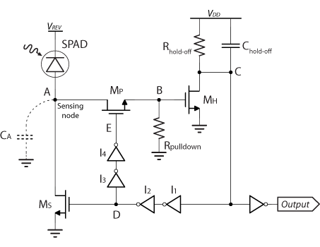
The VLQC circuit is engineered to optimize performance in applications where space and efficiency are critical. The integration of a single transistor for multiple functions simplifies the design and minimizes the number of components, which contributes to the compactness of the overall system. This arrangement not only enhances the reliability of the circuit by reducing potential points of failure but also allows for easier integration into larger systems.
The quenching process is vital in ensuring that the detector can reset rapidly after a photon detection event, thus enabling it to be ready for the next event without significant downtime. The low afterpulsing characteristic is particularly important in high-speed applications, as it reduces the likelihood of false signals that can arise from residual charge in the detector.
Moreover, the output buffer plays a crucial role by ensuring that the VLQC can effectively interface with external circuits or pads, providing the necessary drive strength to accommodate various load conditions. The compact design of the VLQC, comparable to a 20µm SPAD, allows for high-density arrangements in sensor arrays, making it suitable for applications such as imaging systems, LIDAR, and other optical detection technologies where space and performance are paramount.
In conclusion, the VLQC represents a significant advancement in quenching circuit design, balancing the need for compactness with the operational requirements of modern detection systems. Its innovative use of a single transistor for multiple roles, combined with a design that minimizes parasitic capacitance, positions it as a leading solution in the field of photodetection.VLQC is a quenching circuit designed in our laboratories to perfectly suit the constraints of an array, i. e. high compactness, cross-talk avoidance and low afterpulsing. In VLQC a single transistor performs the sensing, quenching and reset tasks drastically reducing the overall detector parasitic capacitance and thus system power consumption, pixel-to-pixel optical
coupling and afterpulsing. The picture below shows a test integrated circuit comprising the VLQC. A part from the output buffer that is necessary to drive pads, VLQC area is comparable with a 20um SPAD area. 🔗 External reference
Related Circuits
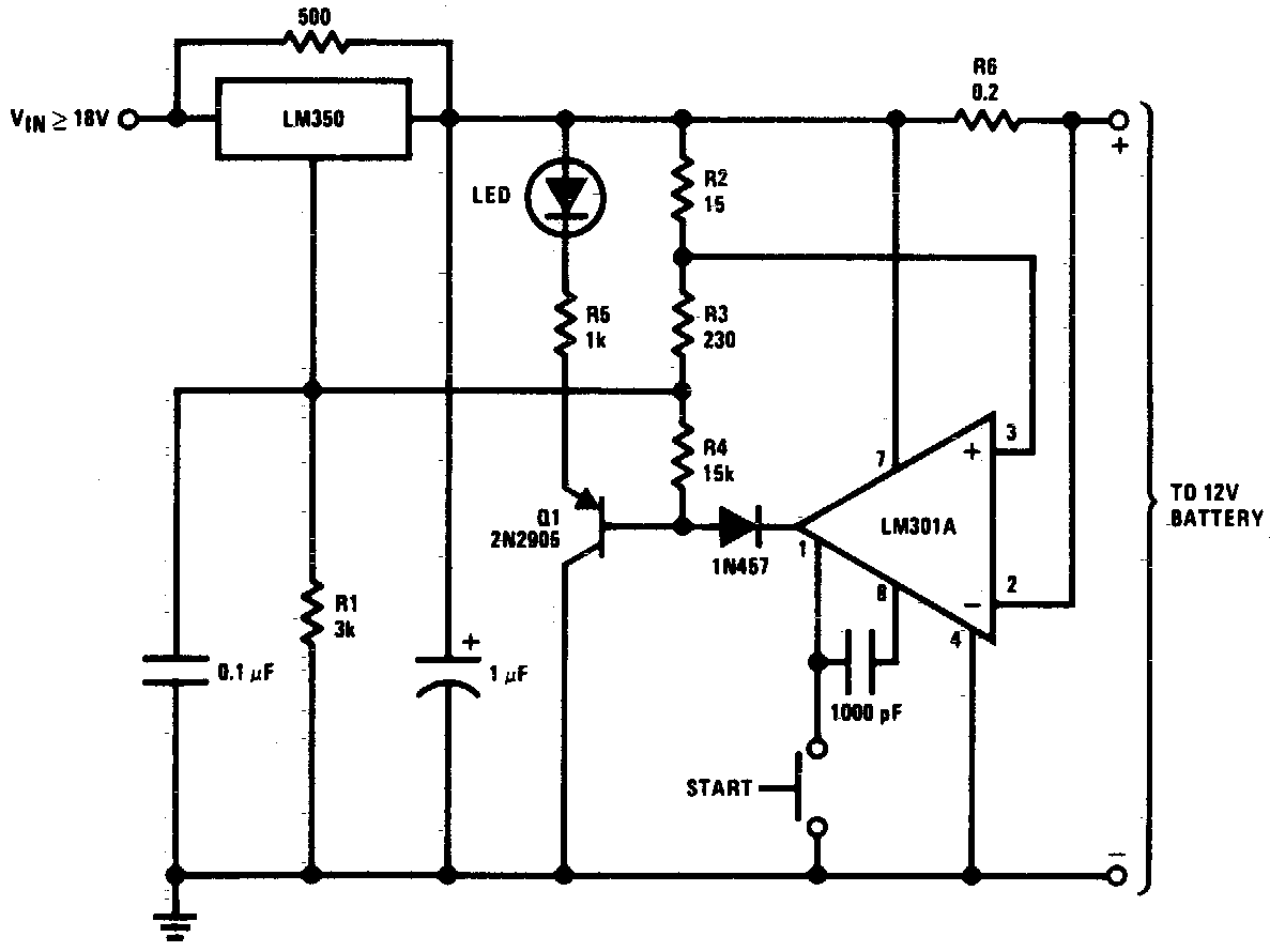
DC 12V Battery Charger Circuit Diagram. This circuit is a high-performance charger for gelled electrolyte lead-acid batteries. The DC 12V battery charger circuit is designed to efficiently charge gelled electrolyte lead-acid batteries, which are commonly used in various applications due...
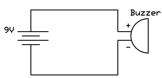
This project involves connecting the positive terminal of the battery to the positive lead of the buzzer and the negative terminal of the battery to the negative lead of the buzzer. Typically, the positive lead of the buzzer is...
This combination sync stripper and universal video interface can solve various problems, including interfacing Super Nintendo with other devices, video overlay, and locking TV frames for scopes. Kits, fully tested units, and custom cable assemblies are available through Redmond...
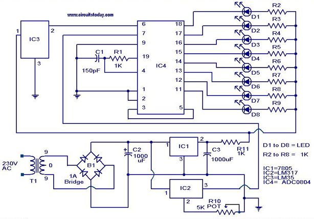
A digital temperature sensor circuit is explained with a circuit diagram. ICs ADC 0804, LM35, and LM317 are used in this digital circuit project. The digital temperature sensor circuit utilizes three primary integrated circuits (ICs): the ADC 0804, LM35, and...
A 35W resistive and capacitive half-wave phase-shift trigger control circuit is designed for automatic or semi-automatic welding equipment to manage wire feeding and welding carriage travel. This system necessitates a drive control circuit to fulfill the welding process requirements....
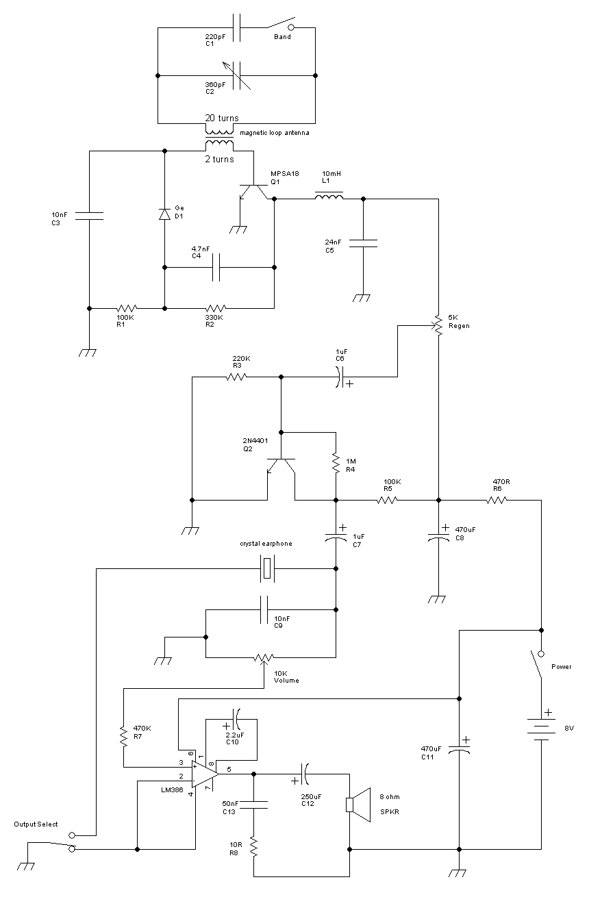
This receiver is a modification of Charles Wenzel's Two Transistor Reflex Radio. Instead of a ferrite AM loopstick antenna, a magnetic loop antenna is used, and an LM386 amplifier stage has been added to drive an 8-ohm speaker. A...
Warning: include(partials/cookie-banner.php): Failed to open stream: Permission denied in /var/www/html/nextgr/view-circuit.php on line 713
Warning: include(): Failed opening 'partials/cookie-banner.php' for inclusion (include_path='.:/usr/share/php') in /var/www/html/nextgr/view-circuit.php on line 713