
Voice link over spread spectrum radio
Wide-band systems can be used paralell with narrow-band systems using th e same frequency. Process gain allows to reduce output power of transmitter. Major methods used in spread spectrum systems are: Rfequency hopping, time hopping, direct sequence or their hybrids. Spread spectrum signals can support any users signal by conventional analogue or digital modulation. However using AM modulation will destroy signals uniform power spectral density, and it will make more difficult to correlate PN sequence in receiver.
Analogue modulated signals are possible to be demodulated without any knowledge of PN code. Frequency modulation is better with frequency hopping spread spectrum. When we use direct sequence spread spectrum, the most suitable will be digital modulation of PN code. We used bipolar phase shift keying. Analogue acoustic signal is converted to digital. Digitalised voice is EX-ORed with digital PN (pseudo-noice) sequence. Modified PN code drives DBM (double balanced mixer) configured as biphase shift keyer. (spreading spectrum). After amplification goes to antenna. In receiver wideband signal arter amplification is EX-Ored with original PN code (despreading spectrum).
Narrow-band signal is BPSK modulated. After demodulation, digitalized voice is converted to analog. Main condition is to know PN code, its frequency and phase with precision better than ½ byte. o synchronisate PN codes three identical channels are used. Except main branch, we have 2 additional branches. Signal in LATE branch is EX-Ored with PN code which is delayed compare to PN code used in main branch about 1 byte. Signal in EARLY branch is EX-Ored with PN code which is earlier than main PN code about 1 byte. When frequency of PN generator in receiver is lower than in transmitter, we receive peak RSSI LATE in LATE branch.
When frequency of PN generator in receiver is higher than in transmitter, we receive peak RSSI EARLY in EARLY branch. Both peaks (RSSI LATE and RSSI EARLY) are used to adjust generator VCXO (4MHz) in receiver. So we have PN generators in transmitter and in receiver have identical frequency and phase. Only in this case is posible to despread spectrum and receive narrow-band signal BPSK in receiver. As a analog to digital (A/D) converter sigma-delta modulator is used. The sampled values of audio signal is compared with staircase approximation of output signal. If the sampled waveform exceeds the staircase approximation, 1 is generated. If the sampled waveform is less than the staircase approximation, 0 is generated. This pulses (0s or 1s) are digitalized voice. When we look at waveform of analog signal, after delta modulator we receive 1s when analog signal increases and we receive 0s when analog signal decreases.
When we have constant value or there is no signal, on output of delta-sigma modulator we receive 01010101010101. alternate. At the receiver, the transmitted pulses are integrated and passed through a low-pass filter. The output of BPSK demodulator does not recover original data polarity. We receive stream of bits identical or inverted compare to original digitalized voice stream in transmitter.
In long time transmission, the polarity of digital signal can change a few times, because of disturbations of work of BPSK demodulator. Because as a digital to analog (D/A) converter we use integrator and low-pass filter, change of digital signal from BPSK demodulator causes only change phase of audio output signal.
We can not hear it, It is why the polarity recover is no needed in receiver. The crystal oscillator supplies sinus 16MHz to digital part add sinus 48MHz to make a carrier frequency. Signal 48MHz is multiplied x4 and amplified. Sinus carrier 192 MHz is coming to DBM (double balanced mixer) configured as biphase shift keyer. Carrier is spreaded by modified PN sequence (spreading spectrum). Spreaded signal after amplification goes to antenna. 16MHz signal from crystal oscillator goes to binary divider. After divider we receive 62. 5kHz to sampling delta-sigma modulator and 4MHz to provide PN generator. PN generator is made of shift register 74HC164 and EX-OR gates 74HC86. PN sequence is EX-Ored with digitized audio. Modified PN spreading code drives DBM to spread carrier 192MHz. Connecting to GND of inputs of NAND gates causes transmitter generates narrow-band BPSK signal or transmitter generates non modulated carrier 192MHz.
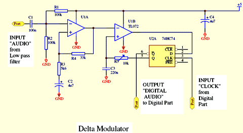
Audio signal after amplifier is send to limiter and low-pass filter. Delta-sigma modulator converts audio into serial data stream. This 1-byte A/D converter is made of trigger 74HC74 and operational amplifier configured as comparator. Audio signal in delta-sigma modulator is sampled by 62. 5kHz signal taken from binary divider. Binary stream (digitized audio) from delta modulator goes to EX-OR gate to modify PN code. Signal from microphone is amplified and next his dynamic is compressed (fig. 2). After amplification by T1 through variable divider signal goes to output amplifier T3 and T4. Divider consist of resistor 22k and T2. It`s attenuation depends on voltage on capacitor 47 µ. Output signal from T4 is rectified and charges capacitor 47 µ. When amplitude of output signal increases, capacitor 47 µ is charged more, and increases attenuation inserted by variable divider (resistor 22k and T2).
It causes decreasing amplitude of output signal. When amplitude of output signal decreases, capacitor 47 µ is charged less, and decreases attenuation inserted by variable divider. It causes increasing amplitude of output signal. Small - amplitude signals are amplified more than big - amplitude signals. On the output of T4 we have audio signals with approximate constant amplitude. From T4 signal goes to low pass filter made of T5 and T6. It limits audio spectrum up to 3 kHz with decline 8x/oct. Coupling capacitors 0. 1 µ limit audio spectrum down to about 30 Hz (fig. 2). After limiter and low-pass filter audio signal is amplified by first operational amplifier (fig. 3). We adjust resistor 5k6 to reach maximum amplitude of audio signal without distorsions. Second operational amplifier configured as comparator. It compares sampled values of signal with a staircase approximation of output signal (taken from capacitor 0.
22 µ). We adjust variable resistor 4k7 to minimum distorsions. If the sampled waveform exceeds the staircase approximation (signal increases), from output of comparator is taken 1 ” to input of trigger 74HC74. If the sampled waveform is less than the staircase approximation (signal decreases), from output of comparator is taken 0 ” to input of trigger.
Signal clock 62. 5kHz for sampling is taken from binary divider (showed on fig. 4). If there is no audio signal, 1s and 0s are generated alternate. In this case we have digital signal 31. 25kHz (fig. 3) Delta-sigma modulator converts audio into serial data stream which goes to digital part of transmitter (showed on fig. 4). Signal from 16MHz generator (from fig. 5) after buffer (first NAND gate) goes to binary divider 74HC4040. After dividing by 256 we receive signal 62, 5 kHz for sampling audio (in delta-sigma modulator fig. 3). 16 MHz after dividing by 4 is 4 MHz to drive PN (pseudo noise) generator. Generator PN is made of 8-stage shift register 74HC164 and EX-OR gates 74HC 86 in feedback circuit. We use 7 registers. It allows to generate PN code of 127 bytes length. PN sequence goes to second NAND gate. Connecting to GND of its second input causes transmitter generates narrow-band BPSK signal. PN sequence (if second input of NAND gate is not grounded) goes to EX-OR gate. To the second input of this EX-OR gate goes binary stream (digitized audio) from delta modulator (showed on fig.
3). This EX-OR gate modifies PN sequence in this way: it inverts PN sequence if digitized audio value is 1 ”. If digitized audio value is 0 ”, passes PN code with no changes. Modified PN sequence goes to third NAND gate. Connecting to GND of its second input causes transmitter generates non modulated carrier. Both switches S1 and S2 can be helpful during testing. Using S2 and generate carrier only helps to adjust RF part of transmitter and downconverter in receiver.
Using S1 (S2 not used) we have narrow-band BPSK signal which may help to adjust BPSK demodulator in receiver. Fourth NAND gate configured as inverter inverts modified PN sequence. Both signals WY ” and /WY ” through resistors k68 drive double balanced mixer configured as BPSK modulator (showed on fig.
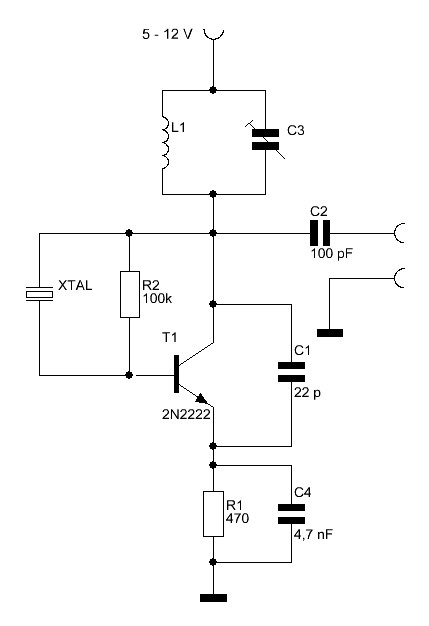
5). Oscillator with T1 (fig. 5) is stabilized by crystal Q=16 MHz. From emiter of T1 signal 16 MHz goes to amplifier-limiter with T5. From its output square - wave signal 16 MHz goes to buffer before binary divider in digital part (showed on fig. 4). LC circuit in collector of T1 is tuned to frequency 48 MHz. This signal goes to multiplier x4 with T2. LC circuit in collector of T2 is tuned to frequency 192 MHz. From its output signal is taken to buffer 192 MHz with T3. Sinus signal 192 MHz (carrier) is phase modulated by double balanced mixer configured as BPSK modulator.
(spreading spectrum by modified direct PN sequence). Double balanced mixer is driven through resistors k68 by signals WY and /WY from digital part (showed on fig. 4). On the output of mixer we have signal with spread spectrum. 90% of its energy has bandwidth 8 MHz: from 188 MHz to 196 MHz (carrier frequency +/- clock frequency of PN generator).
SS signal through buffer with T4 goes to output. This signal can be amplified by power amplifier (not showed). Power amplifier must have bandwidth minimum 8 MHz. 🔗 External reference
Related Circuits
Crystals with higher frequencies than approximately 30 MHz are predominantly overtone crystals. These crystals are designed to operate at an odd multiple of their fundamental frequency. However, they do not resonate at their overtone frequency without assistance; the oscillator...
The SciSys Leonardo, Saitek Galileo, and Renaissance chess computers can be connected to a PC using an OSA-Link cable, which is necessary to operate the OSA-4-Arena software and other tools. However, this cable is no longer available. Detailed instructions...
This version of the Link is intended for users who require an affordable and reliable intercom system without access to an external telephone line. It is suitable for environments such as preschools, hobby farms, or small workshops and factories,...
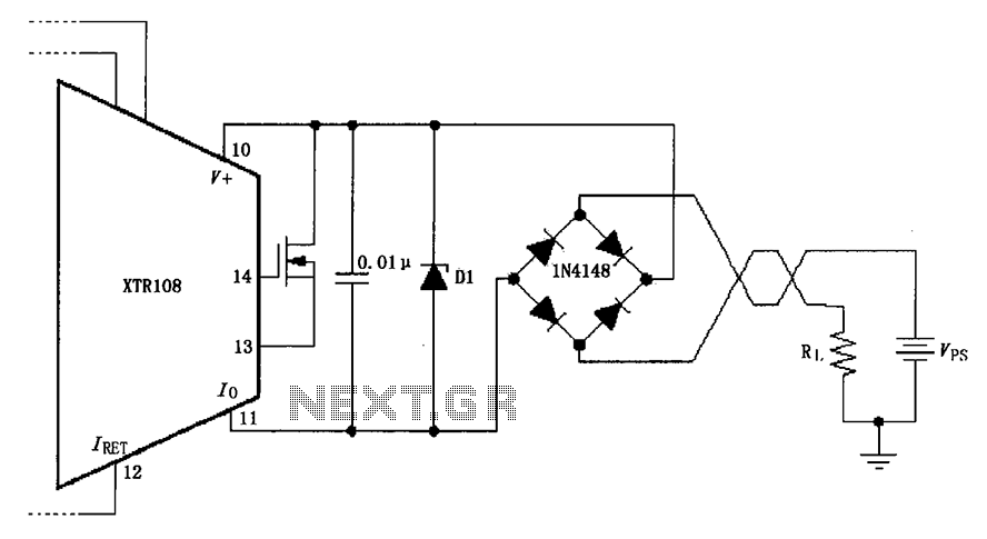
The circuit utilizes a Zener diode (D1) for overvoltage protection and a diode rectifier bridge for reverse voltage protection. The 1.4V drop across the diodes will result in a maximum voltage loss, meaning that the supply voltage (VPS) must...
A clock-and-data recovery (CDR) circuit is utilized to recover the clock from a transmitted data stream and re-time that data with the recovered clock. These circuits are generally positioned at the front-end of receiver chips to extract the clock...
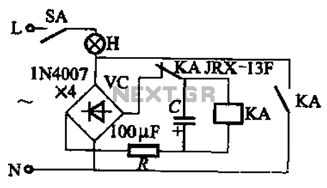
The circuit illustrated in Figure 13-3 consists of two configurations: (a) a DC power supply and (b) an AC power supply. Both configurations are utilized to control a relay. The flash frequency of the relay is determined by the...