
Voltage Level Translator
The described low noise amplifier (LNA) is engineered for various applications across a broad frequency range, making it highly versatile for RF design. The 900 MHz ISM band and satellite communications are among the key applications, where low noise figures are essential for maintaining signal integrity and overall system performance. The BFR740L3RH transistor, characterized by its ultra-low noise figure and high gain, plays a pivotal role in achieving the desired amplification while minimizing signal degradation.
The TSLP-3-9 package design is particularly advantageous for compact applications, as it allows for integration into space-constrained environments. With dimensions of 1 x 0.6 x 0.4 mm, the package supports high-density PCB layouts, which is critical in modern electronic designs. The use of 0201 passive components further enhances the compactness of the circuit, ensuring that the footprint of the LNA remains minimal while still delivering optimal performance.
In terms of performance, the LNA is designed to operate efficiently over a frequency range of 200 MHz to 6 GHz, making it suitable for various wireless communication standards, including WLAN (802.11 b/g/a) and satellite radio. The feedback mechanism incorporated in the design helps to stabilize the gain across the operating frequency range, providing consistent performance and improving linearity.
Overall, this low noise amplifier presents a robust solution for applications requiring high performance in a compact form factor, making it an excellent choice for engineers looking to optimize their RF designs. The careful selection of components and the innovative packaging contribute to the amplifier's effectiveness in diverse communication systems.Applications 900 MHz ISM Band, Satellite TV LNB IF Amplifiers (950 - 2150 MHz), 1575 MHz GPs 2. 4 GHz ISM Band (802. 11 b/g WLAN, Cordless, etc. ), "SDARS" Satellite - based Radio (2. 33 and 2. 6 GHz), 5 - 6 GHz WLAN (802. 11a), 5 GHz Cordless Phones, etc. Overview A Wideband, Feedback Low Noise Amplifier (LNA) for 200 MHz to 6 GHz, using the Ultra Lo w Noise BFR740L3RH RF Transistor in TSLP-3-9 Leadless Package with a height of only 0. 32 mm. The Silicon-Germanium BFR740L3RH B7HFe Ultra-Low-Noise RF Transistor is shown in a simple, low-cost general-purpose wideband LNA application. 0201 case size passive components are used to reduce occupied PCB area. The BFR740L3RH TSLP-3-9 package is only 1 x 0. 6 x 0. 4 mm, and is suitable for use in modules. The complete Amplifier only uses 16 mm ² of PCB area. 🔗 External reference
Related Circuits
The charging circuit features adjustable voltage output settings, allowing for regulation of the charging voltage supplied to the battery. The use of a potentiometer facilitates precise voltage management, with adjustments possible down to the millivolt range. Refer to the...
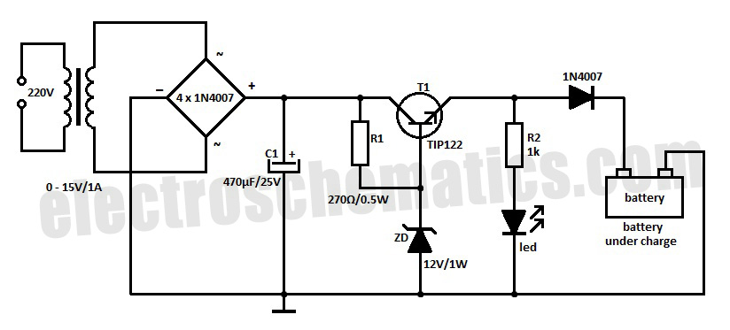
Most battery chargers lack provisions for current and voltage regulation. The step-down voltage is primarily utilized for charging purposes. Many battery chargers operate on a straightforward principle of reducing the input voltage to a level suitable for charging a battery....

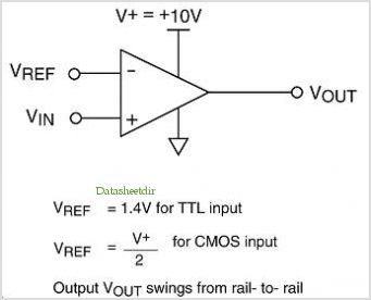
This circuit is designed as a low-cost voltage reference. Its main component is a general-purpose operational amplifier, the 741, configured to output a buffered fixed reference voltage for use by other integrated circuits or circuits, such as an Analog-to-Digital...
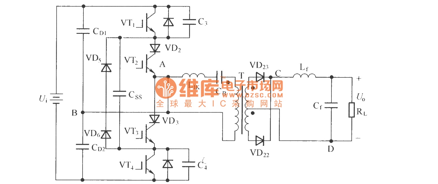
To eliminate circulating current in a zero-voltage switch three-level DC converter during its zero state, a zero-voltage zero-current switch three-level DC converter circuit has been proposed. The primary distinction between this circuit and the standard zero-voltage switch three-level DC...
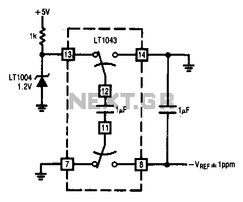
This circuit enables the inversion of a reference signal with an accuracy of 1 ppm. It features high input impedance and does not require any trimming. The described circuit is designed to invert a reference voltage signal while maintaining a...
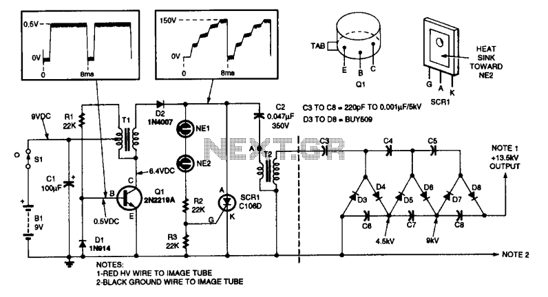
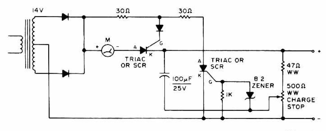
This high-voltage power supply features an inverter circuit centered around Q1, which generates 150-V pulses for the converter SCR1 and capacitor C2. The output from component ?2 produces a 4.5-kV pulse, which is further amplified by a voltage-tripler network...