
Voltage-ratio-to-frequency-converter
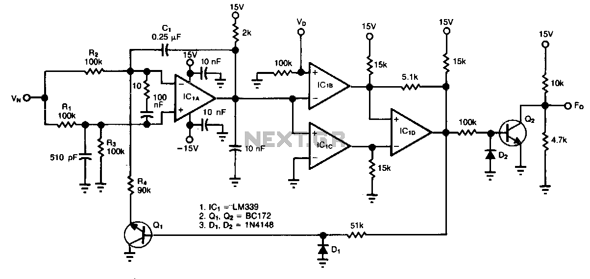
The circuit accepts two positive voltage inputs, VN and Vv, and provides a TTL-compatible output pulse train whose repetition rate is proportional to the ratio VN/V0. The full-scale output frequency is approximately 100 Hz, and the linearity error is below 0.5 percent. The output frequency, F, is equal to KVn/Vd, where K = 1/(4R2C1), provided that R1 = R3. Operational amplifier IC1A alternately integrates VN/2 and -VN/2, producing a sawtooth output that ramps between the Vv level and ground. When transistor Q1 is on, for instance, IC1A integrates -VN/2 until its output equals Vv. At that moment, the IC1B comparator switches low, causing the output of IC1D to go low, which turns off Q1. The output of IC1A then ramps in the negative direction. When the output reaches 0 V, the IC1C comparator switches, Q1 turns on, and the cycle repeats. Transistor Q2 converts the output of IC1D to TTL-compatible output logic levels. Setting Vv to 1.00 V yields a linear voltage-to-frequency converter (F = KVn), and setting VN to 1.00 V yields a reciprocal voltage-to-frequency converter (F0 = KVd).
The described circuit functions as a voltage-to-frequency converter utilizing operational amplifiers and transistors to produce a stable output pulse train based on the input voltage levels. The architecture consists of two main operational amplifiers, IC1A and IC1B, which are configured to perform integration and comparison tasks, respectively. IC1A operates by integrating the input signals, generating a sawtooth waveform that oscillates between the defined voltage levels, Vv and ground.
The integration process involves alternating between integrating VN/2 and -VN/2, effectively creating a triangular signal that can be used for further processing. The output of IC1A is monitored by comparator IC1B, which detects when the integrated value reaches the threshold defined by Vv. Upon reaching this threshold, IC1B triggers a state change in the bistable flip-flop IC1D, which controls the state of transistor Q1.
Transistor Q1 plays a critical role in regulating the integration cycle. When Q1 is activated, it allows the integration to proceed until the output from IC1A matches Vv. Once this condition is met, the comparator IC1B transitions low, which in turn deactivates Q1 and allows the output of IC1A to decrease. This negative ramp continues until the output reaches 0 V, at which point comparator IC1C activates Q1 again, restarting the integration cycle.
Transistor Q2 serves to convert the output from the flip-flop IC1D into TTL-compatible logic levels, ensuring that the output pulse train can interface effectively with digital circuits. The design allows for flexibility in setting the output frequency based on the input voltages. By configuring Vv to 1.00 V, the circuit operates as a linear voltage-to-frequency converter, where the output frequency directly correlates with the input voltage VN. Conversely, setting VN to 1.00 V transforms the circuit into a reciprocal voltage-to-frequency converter, allowing for a wide range of applications in frequency modulation and signal processing tasks. The linearity error of less than 0.5 percent ensures reliable performance across the specified operational range.The circuit accepts two positive-voltage inputs VN and Vv and provides a TTL-compatible output pulse train whose repetition mte is proportional to the ratio VN/ V0. Full-scale output frequency is about 100 Hz, and linearity error is below 0.5 percent. The outputF, equals KVn/Vd, where K = 1/(4R2C1) provided R1 = R3. Op amp IC1A alternately integrates VN/2 and -VN/2, producing a sawtooth output that ramps between the Vv level and ground.
When transistor Ql is on, for example, IC1A integrates -VN/2 until its output equals Vv. At that time, the IC1B comparator switches low, causing IClD"s bistable output to go low, which turns off Ql. !CIA"s output then ramps in the negative direction. When the output reaches 0 V, the IC1C comparator switches, Ql turns on, and the cycle repeats. Transistor Q2 converts the IC1D output to TTL-compatible output logic levels. Setting Vv to 1.00 V yields a linear voltage-to-frequency converter (F, = KVn), and setting Vn to 1.00 V yields a reciprocal voltage-to-frequency converter (F0=KVd).
🔗 External reference