
Voltage-to-requency-converter
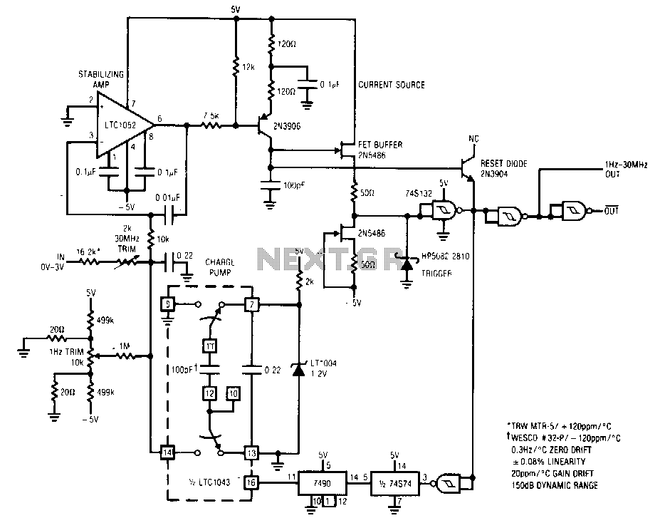
The circuit features a 1 Hz to 30 MHz output with a dynamic range of 150 dB, designed for a 0 to 5 V input. It exhibits a linearity of 0.08% across its entire 71/3 decade range, with a full-scale drift of approximately 20 ppm/°C. To achieve the additional bandwidth, a fast FET buffer is employed to drive a Schottky TTL Schmitt trigger. The Schottky diode ensures that the Schmitt trigger does not encounter negative voltages at its input. The hysteresis of the Schmitt trigger's input voltage establishes the operational limits for the oscillator. The 30 MHz full-scale output exceeds the LTC1043's input capabilities; therefore, digital divider stages are utilized to attenuate the feedback frequency signal by a factor of 20. The remaining Schmitt sections provide complementary outputs.
The described circuit is a versatile signal processing unit capable of generating outputs across a wide frequency range, specifically from 1 Hz to 30 MHz. The dynamic range of 150 dB indicates exceptional performance in terms of signal fidelity and noise rejection, making it suitable for high-precision applications. The linearity specification of 0.08% signifies that the output signal closely follows the input within the specified range, ensuring reliable performance across various operating conditions.
The inclusion of a fast FET buffer is crucial for enhancing the bandwidth of the circuit. FETs are known for their high input impedance and low output capacitance, which contributes to the rapid signal processing capabilities required for high-frequency applications. The Schottky TTL Schmitt trigger plays a vital role in shaping the output waveform, providing fast switching times and ensuring that the circuit can handle high-speed signals without distortion.
The Schottky diode serves as a protective measure, preventing any negative voltage spikes from reaching the Schmitt trigger's input. This protection is essential for maintaining the integrity of the signal and ensuring the longevity of the components involved. The hysteresis characteristic of the Schmitt trigger is particularly beneficial, as it defines the threshold levels for the oscillator's operation, thus stabilizing the output and minimizing the effects of noise.
The use of digital divider stages to attenuate the feedback frequency signal by a factor of 20 is a strategic design choice. This step allows the circuit to operate within the acceptable input range of the LTC1043, which is critical for maintaining accurate signal processing while preventing overload conditions. The complementary outputs provided by the remaining Schmitt sections enhance the versatility of the circuit, allowing for various applications where both positive and negative signal swings are required.
In summary, this circuit design demonstrates a sophisticated integration of components that collectively ensure high-speed performance, robust signal integrity, and adaptability for a wide range of electronic applications.Circuit has a 1 Hz-to-30 MHz output, 150-dB dynamic range, for a 0 to 5 V input. It maintains 0.08% linearity over its entire 71/3 decade range with a full-scale drift of about 20 ppm/°C. To get the additional bandwidth, the fast )FET buffer drives the Schottky TTL Schmitt trigger. The Schottky diode prevents the Schmitt trigger from ever seeing negative voltage at its input. The Schmitt"s input voltage hysteresis provides the limits which the oscillator runs between. The 30-MHz, full-scale output is much faster than the LTC1043 can accept, so the digital divider stages are used to reduce the feedback frequency signal by a factor of 20. The remaining Schmitt sections furnish complementary outputs. 🔗 External reference