
Water Activated Relay circuit board
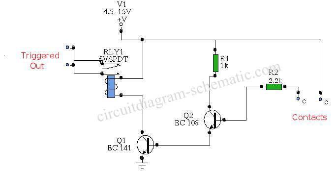
The water-activated relay circuit utilizes a simple yet effective design to control devices based on the presence of water. The primary components include two transistors, which serve as the core amplification elements. The first transistor (T1), a 2N2222A, is configured in a common-emitter arrangement, providing a significant voltage gain and enabling the circuit to respond to low currents generated by water flow. The second transistor (T2), also a 2N2222A or a BC108, operates in a similar manner, enhancing the overall current gain of the circuit.
The circuit is powered by a DC voltage supply, typically set at 5 volts for optimal performance. This voltage level is sufficient to drive the relay, which generally requires a current of 60 mA to engage its switching mechanism. The relay serves as the output device, allowing the circuit to control larger loads, such as lights or pumps, based on the water detection input.
The water detection mechanism relies on the conductivity of water, which allows a small current to flow through the circuit when water is present. This current is sufficient to bias the transistors into their active regions, enabling them to amplify the current and ultimately energize the relay coil. The threshold for activation is set at a minimum of 4 microamperes, which can be easily achieved with common sources of water, such as tap water or rainwater.
In summary, this water-activated relay circuit is a practical solution for applications requiring automatic control based on water presence. Its design leverages the high gain characteristics of the transistors to ensure reliable operation with minimal water flow, making it suitable for various environmental monitoring and automation tasks.Circuit diagram is water activated relay circuit. In this diagram circuit using two transistors connected as a high gain compound pair. 2N2222A transistors T1 and T2 may be a BC108. Current gain will be the product of each transistor beta, which will be a minimum of 140 x 110 or 15, 400. Power supply voltage can be used 4, 5-15 volts, a typical 5-vo lt relay may require 60 mA to operate, in this case any fluid flow through at least 4 UA will activate the relay. This is easily achieved with tap or rain water. The following is a schematic drawing: 🔗 External reference
Related Circuits
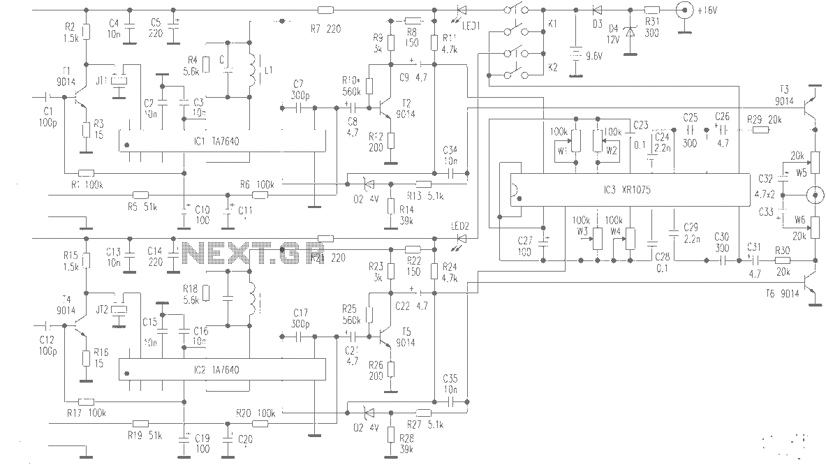
The production of high-quality wireless microphones is a common aspiration among enthusiasts, but achieving a high-performance receiver is challenging. This project explores the use of salvaged FM radio cassette players to enhance an XR1075 audio processor, leading to the...

The device is a DC switch that remains normally on due to the forward biasing of Q1 through resistor R3. Q1 clamps Q2 into a forward state by biasing its complementary transistor well into saturation via resistor R4. The...

The purpose of this circuit is to maintain a permanent magnet DC motor at a constant speed, which is set externally. This is achieved by monitoring the current flowing through and the voltage across the motor's brushes. The schematic for...
It is advisable to prototype the entire circuit using a breadboard. This method simplifies the process significantly compared to attempting to determine the connections on a small printed circuit board. Prototyping a circuit on a breadboard allows for easy modifications...
The circuit depicted in the figure allows for the selection of optimal operating conditions and a suitable allocation of the temperature coefficient for the resonant circuit components. The resonance occurs at both ends of the circuit. Additionally, the exchange...

The circuit can incorporate a buffer gate at the input to ensure compatibility with TTL or other logic levels. This design is intended for a TTL 0V circuit to accommodate a 3.5V input signal swing. Additionally, it generates a...