
Wide Frequency Range 555 VCO
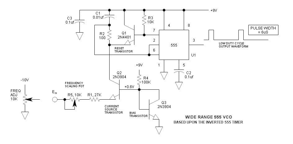
The described circuit utilizes the 555 timer in an inverted configuration to enhance frequency modulation capabilities. The inclusion of Q2 in a common base configuration allows for improved linearity in the charging process of capacitor C1. The choice of a negative supply voltage for the emitter is crucial, as it enables the circuit to maintain functionality across the specified frequency range. The scaling of frequency via R5 is a critical design aspect, ensuring that the output frequency remains within the desired parameters for practical applications.
The self-biasing arrangement of Q3 is an innovative approach that simplifies biasing requirements while maintaining stable operation. The calculated emitter current and the relationship between the resistances and voltage drops are fundamental to achieving the desired performance. The use of the 2N4401 transistor is particularly noteworthy, as it offers a higher current gain at elevated current levels, making it suitable for applications requiring robust performance.
The circuit's performance is characterized by its linearity and the potential for minimal offset errors, although practical limitations exist due to component tolerances and the inherent characteristics of the 555 timer. The careful selection of components, including the resistor values and transistor types, plays a significant role in optimizing the overall circuit behavior. This design exemplifies the balance between theoretical ideals and practical engineering considerations in electronic circuit design.The 555 frequency can be varied via adjusting the voltage at pin 5. However, the range and linearity of frequency adjustment is very limited. This is a way to greatly improve performance using the inverted 555 timer circuit that was previously posted. Q2 is connected in the common base configuration. In this mode of operation, the collector curren t is a function of emitter current regardless of the collector voltage. In this way, it can perform a linear charge function upon C1. The emitter must be driven from a negative supply voltage. Frequency is scaled to 10V = 10kHZ via R5. Frequency range in this set-up is 180 to 10kHZ. Q3 is wired as a self-biasing transistor by connecting the base to the collector and feeding it a bias current via R4. Voltage drop is 0. 6V. Originally, I had a 1N4148 diode and its voltage drop was 0. 45V that added too much offset to the emitter of Q1. Ideally, the voltage drop across Q3 should equal Vbe of Q2. This is a compromise because they are matched only under the condition of Ie = (9V 0. 6V) /R4 = 84uA. The emitter current varies from about 3 to 303uA. Lowest low end offset would occur with both transistors matched and R4 increased to 3M ”in that case, the hFE @ 3uA must >100 ”this looks practical, but would require a different transistor selection ”I did not experiment with this option.
Q1 is a 2N4401. It varies from the 2N3904 in that its current gain (hFE) is optimized at a higher current. The reset current must be high due to its low duty cycle. Linearity is shown over two orders of magnitude. While not perfect, it shows how the circuit performs. The error on the low end is caused by input offset voltage that is not perfectly nulled via the voltage drop of Q3. On the high end, non-linearity is caused by the finite reset time of the 555 that runs about 6% @ 10kHZ.
🔗 External reference
Related Circuits
This project uses a four-point resistance measurement process also known as the Kelvin method. This procedure uses a current source to determine the value of an unidentified resistance. A constant current flows through the unknown resistance and the voltage...
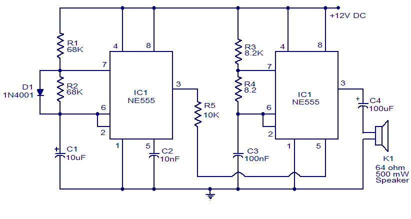
A variety of electronic circuits utilize the NE555 timer integrated circuit (IC). The circuit diagram presented illustrates a police siren based on two NE555 timer ICs, both configured as astable multivibrators. The circuit operates on a DC voltage supply...
Some simple 555 and flip-flop circuits are being developed to add electronic lighting effects to modernize games. Various circuits are being collected for different game aspects, such as idle states, flipper shots, flower openings, winning shots, etc. A collection...
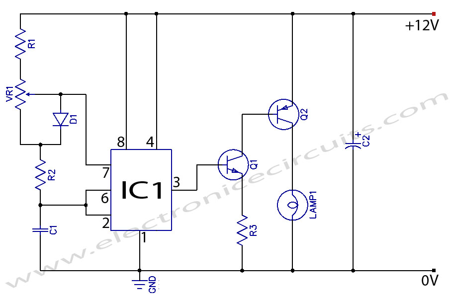
When the potentiometer is in the upper position, the capacitor charges rapidly through both 1k resistors and the diode, resulting in a brief positive interval and an extended negative interval, which dims the lamp to near darkness. Conversely, when...
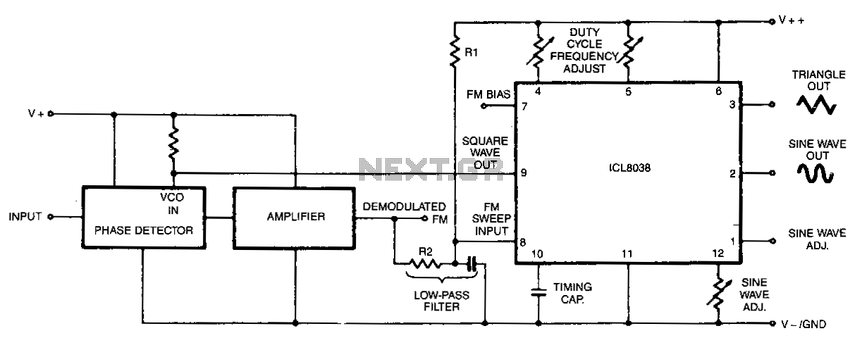
In this circuit, a waveform generator is used as a stable voltage-controlled oscillator (VCO) in a Phase-Locked Loop (PLL). The circuit utilizes a waveform generator configured as a voltage-controlled oscillator (VCO), which is a critical component in the design of...
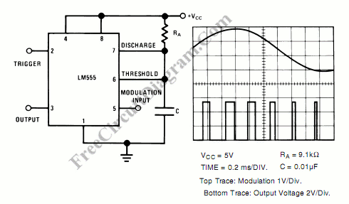
A pulse width modulator generates a PWM signal, which consists of pulses with a constant frequency while the duty cycle varies according to a modulating signal. A pulse width modulator (PWM) is an essential component in various electronic applications, particularly...
Warning: include(partials/cookie-banner.php): Failed to open stream: Permission denied in /var/www/html/nextgr/view-circuit.php on line 713
Warning: include(): Failed opening 'partials/cookie-banner.php' for inclusion (include_path='.:/usr/share/php') in /var/www/html/nextgr/view-circuit.php on line 713