
Wide-range-voltage-to-frequency-converter

This circuit utilizes a programmable operational amplifier, specifically the HA2730, which is a two-amplifier monolithic chip featuring independent programming ports for each amplifier. The parameters of the amplifiers, including the slew rate, vary linearly based on a set current. In this configuration, one amplifier, designated as A1, functions as a slewing amplifier, while the other amplifier, A2, serves as a comparator. The control voltage, Vc, regulates the slew rate of A1. Since A1's output voltage swing remains constant, modulating its set current directly influences the frequency of the circuit. The internal compensation capacitor of A1 acts as the timing component, while an internal bipolar current source, whose magnitude is proportional to the set current at pin 1, determines the charge-discharge rate. The circuit can achieve a conversion nonlinearity of ±0.03% of full scale over three decades and ±1.5% of full scale over 4.3 decades of frequency. The frequency range can be adjusted by modifying the resistance, R.
The HA2730 operational amplifier is designed for applications requiring high precision and flexibility in signal processing. The two amplifiers within the chip allow for distinct functionalities: A1, as the slewing amplifier, is responsible for managing the rate of change of the output signal, which is crucial in applications where fast response times are necessary. The slew rate can be fine-tuned using the control voltage Vc, enabling precise control over the amplifier's performance characteristics.
A2, acting as a comparator, provides a means to compare the output of A1 against a reference voltage, facilitating the detection of specific voltage levels within the circuit. This dual-functionality allows the circuit to perform complex signal processing tasks, such as waveform shaping or frequency modulation, with minimal external components.
The internal compensation capacitor within A1 is critical for establishing the timing characteristics of the circuit. Its value, combined with the set current, defines the charge and discharge rates, directly influencing the frequency response of the system. The bipolar current source ensures that the operational amplifier remains responsive to changes in the set current, maintaining stability and performance across varying conditions.
The specified conversion nonlinearity indicates that the circuit maintains a high degree of accuracy across a wide frequency range, making it suitable for applications that demand precision in signal conversion. The ability to adjust the frequency response by altering the resistance R provides further flexibility, allowing the circuit to be tailored to specific application requirements. This adaptability, combined with the inherent precision of the HA2730, makes this circuit an excellent choice for advanced electronic signal processing tasks.This circuit uses a programmable op amp such as the -HA2730-a two-amplifier monolithic chip with independent programming ports for each amplifier-whose slew rate and other parameters vary linearly with a so-called set current. The converter circuit uses one amplifier, Al, as a slewing amplifier and other, A2, as a comparator function.
The control voltage Vc. determines Al"s slew rate. And, because Al"s output voltage swing is constant, the modulation of its set current results in direct control of the circuit"s frequency. Al"s internal compensation capacitor acts as the timing component. An internal bipolar current source,whose current magnitude is directly proportional to the set current of pin 1, then determines the charge-discharge rate.
A conversion nonlinearity of ±0.03% of full scale over 3 decades and ±1.5% of full scale over 4.3 decades of frequency is possible. The frequency range is adjustable by a change in the resistance, R.
Related Circuits
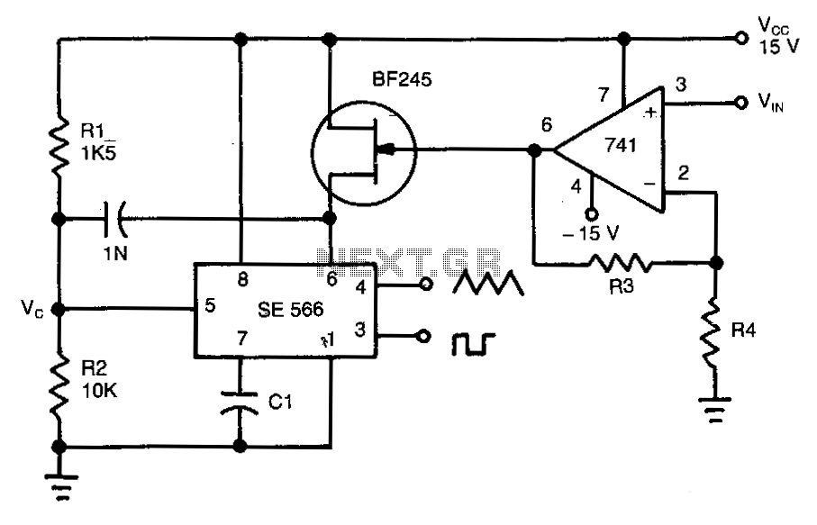
This circuit operates based on the frequency variation of the function generator in relation to the input voltage (ViN). The frequency is influenced by the capacitance and resistor connected to pin 6, with the resistor being substituted by a...